

I cannot believe how fast things are progressing in AI-powered Electronic Design Automation (EDA) space (where no one can hear you scream). AI-enabled EDA tools are popping up like mushrooms for a wide range of design, analysis, and verification tasks. One area that’s seen significant development—and attracted significant skepticism—is the use of AI to place and route printed circuit boards (PCBs).
Following each of my previous AI-powered PCB layout-related columns, I received a lot of pushback from layout designers in the trenches. The two main arguments I’ve heard are that (a) AI tools cannot create layouts for complicated real-world boards as well as experienced humans, and (b) most of the demonstrations involve curated reference designs that are selected to highlight features in the tool. We will address both these points in the tale I’m poised to tell.
I was just chatting with some of the folks at Quilter.ai—specifically, Sergiy Nesterenko (Founder and CEO), Ben Jordan (Product Manager & Technical Marketer), and James Krejcarek (VP of Sales). You may recall my previous Quilter-related column,You May Scoff, But AI-Powered PCB Layout Is Really Real. Well, that was a little more than six months ago, and it’s even more real now.
It turns out the folks at Quilter have been receiving the same pushback I have, so they decided to do something no other AI-powered PCB layout tool has done—create a complete, working single-board computer (SBC)—and they pulled it off with their Speedrun project.
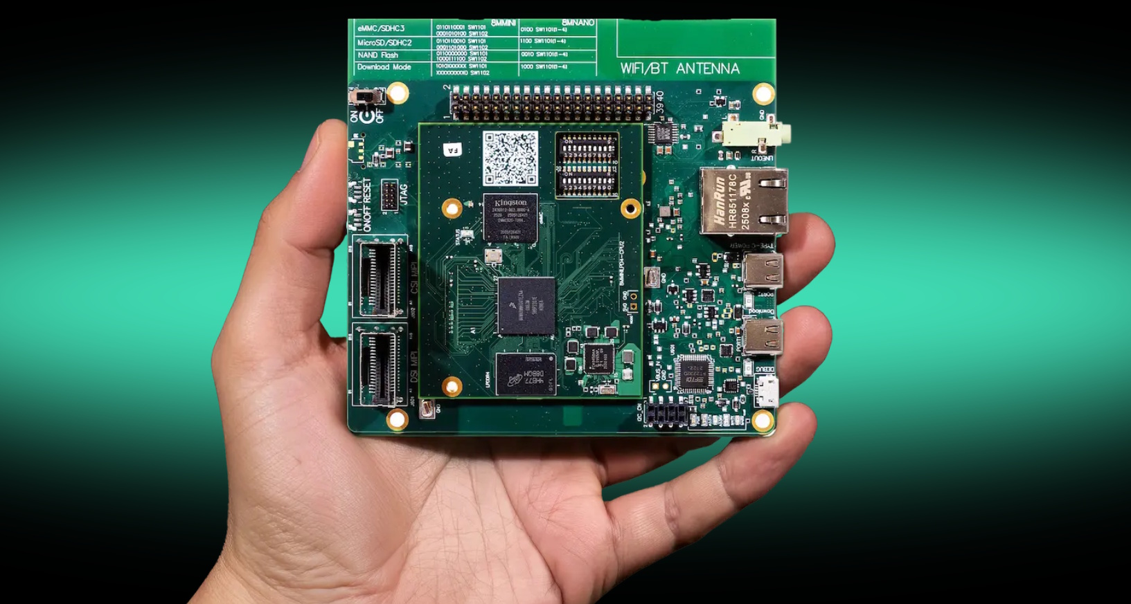
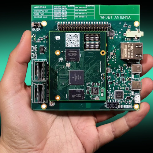
Project Speedrun (Source: Quilter.ai)
Before we delve into this in more detail, let’s first set the scene. Some AI-based EDA companies are trying to do everything. Their vision is that a designer should be able to give an AI a prompt along the lines of, “I want a gizmo that does X, Y, and Z,” and the tool will automatically select the components, generate the schematic, and perform the PCB layout.
The folks at Quilter take a very different view. Based on their experience with
professional design teams, they believe this is not how real-world hardware
development works—at least not in the markets they are targeting. In these
environments, companies want their human design engineers to apply their expertise to architect the system, choose trusted components from vetted libraries, and create the schematic. Quilter’s goal is not to replace those decisions, but to remove one of the most labor-intensive and time-consuming parts of the process—PCB placement and routing.
To prove that this approach works in the real world, the Quilter team knew they needed a serious, non-trivial design—something that would stretch the tool, but without letting peripheral distractions derail the effort. They deliberately chose not to invent a brand-new product from scratch, because that would have meant getting bogged down in driver development, software bring-up, and countless secondary engineering decisions unrelated to PCB layout itself.
Instead, they set their sights on building a single-board computer because (a) this is a design class that is widely understood, (b) it’s inherently challenging from a layout perspective, and (c) it’s easy for others to evaluate. By selecting an existing NXP i.MX 8M Mini reference design, they could leverage a mature processor ecosystem with well-established software support, known-good schematics, and publicly available documentation that anyone can independently inspect and verify.
This choice allowed Quilter to focus squarely on the problem they are trying to solve:automated component placement, routing, stackup selection, and constraint handling. Just as importantly, it gives outside observers something concrete they can inspect, compare, and verify. The resulting boards aren’t theoretical reference designs or marketing demos—they boot, run a browser, and behave exactly as a single-board computer should.
To underline that this is not a toy problem, the team deliberately chose a design that includes LPDDR4 memory. Anyone who has ever laid out a board with high-speed DDR interfaces knows this immediately raises the bar: controlled impedance, tight length matching, power integrity, stackup decisions, and signal integrity constraints all come into play. This was very much a grown-up board.
The project itself naturally splits into two parts: a baseboard and a system-on-module (SOM). This mirrors how many commercial products are built and, crucially, allowed the Quilter team to validate their work in a clean, verifiable way. They could test their SOM on an off-the-shelf NXP baseboard, test the NXP SOM on their own baseboard, and finally run the full Quilter-generated pair together. In every case, the boards behaved exactly as expected.
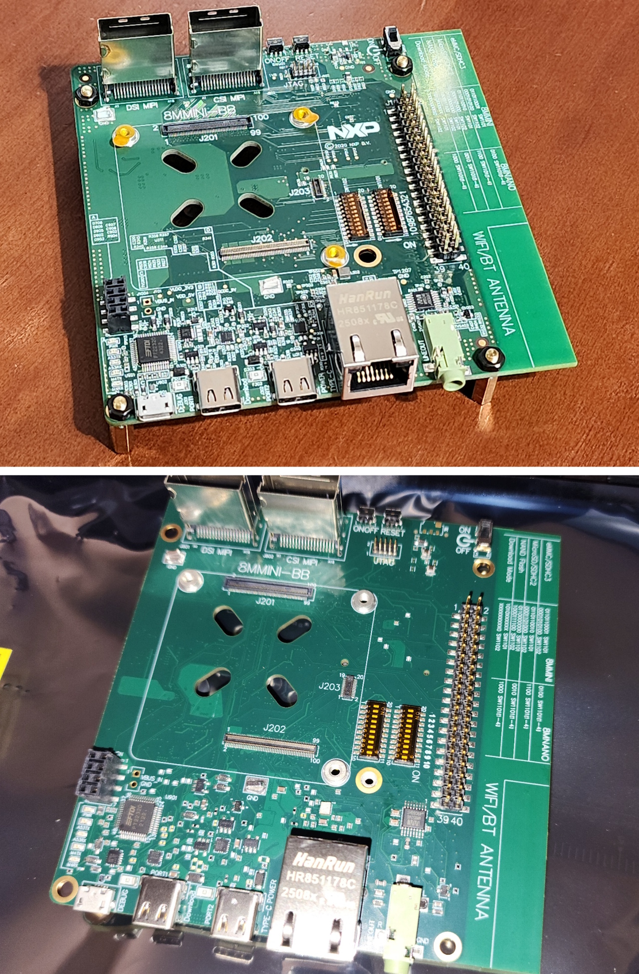
NXP baseboard (top) and Quilter baseboard (bottom) (Source: Quilter.ai)
Quilter SOM mounted on Quilter baseboard (Source: Quilter.ai)
Ben was tasked with making this project happen. He used Altium Designer as his traditional EDA platform because he’s experienced with this environment. However, Quilter can also accept input from other major PCB design platforms such as Cadence Allegro/OrCAD and Siemens EDA (formerly Mentor Graphics), meaning schematics, BOMs, footprints, and constraint files generated in those environments can be handed to Quilter for placement and routing. This interoperability is key for professional teams that already have established libraries and processes in place.
Just as important as what the Quilter team built was how they approached the design. Rather than asking Quilter to conjure a computer from a vague prompt, the team followed the same workflow used by professional engineering organizations. They began by defining the board outline, mechanical constraints, and the exact placement of connectors—details driven by enclosures, cabling, and system integration, not by AI creativity.
This reflects the reality of enterprise-level design. Companies in this space already have the following, none of which is negotiable in a professional environment:
Carefully evaluated processors selected from dozens of candidates
Preferred, qualified components pulled from trusted supply chains
Established schematic designs
Vetted internal libraries with approved footprints
Fixed mechanical constraints dictating board shape and connector locations
All this information was packaged up and handed to Quilter. The AI was not asked to choose parts, invent circuits, or generate footprints. Its job was to do what comes after those decisions have been made: component placement, routing, plane generation, stackup selection, and constraint satisfaction.
Now, I must admit to growing more cynical and more skeptical as the years go by. I’ve seen more than my fair share of carefully curated canned demos and ephemeral vaporware. I must admit to being impressed when the folks at Quilter said how they had tested their SOM in NXP’s baseboard, and vice versa. Also, how they’ve replaced NXP baseboard-SOM combos with their Quilter counterparts in real-world systems, and things have worked perfectly. But still and all…
To allay any lingering doubts I might have, Ben joined our call again. I snapped a screenshot as shown below. One instance shows Ben on his main computer, while the other shows him on his Quilter SBC. “But which is which?” you ask. I no longer recall.
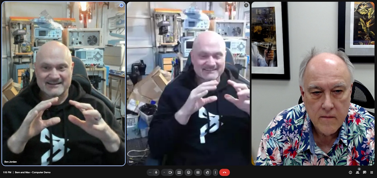
A brace of Bens and your humble narrator (Source: Max Maxfield)
Just to slap a great big dollop of metaphorical cream onto the top of the allegorical cake, Ben set an AI model running on his Quilter SBC while we were talking. Once again, I snapped a screenshot as shown below.
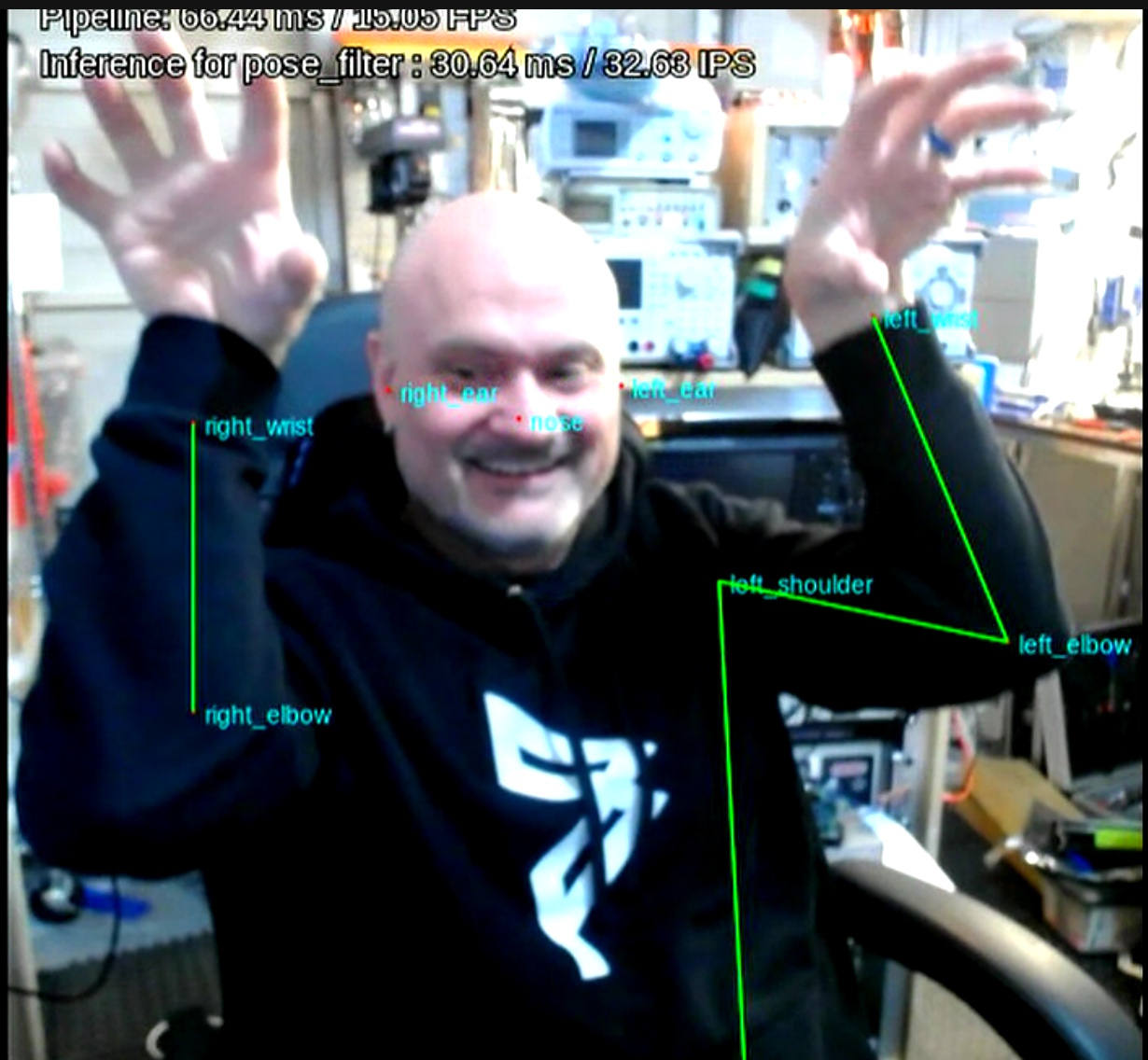
AI model running on the Quilter SBC (Source: Max Maxfield)
But wait, there’s more, because it’s at this point that the story gets particularly interesting. The Quilter team took the exact same design package—the same schematics, BOM, footprints, board outline, and connector placements—and sent it out for quotes from multiple experienced, real-world PCB designers.
The instructions were explicit: assume the schematic is final and known-good, and quote only for placement and routing, exactly as you would for a commercial customer. Those quotes came back at roughly 200 hours per board (400 hours total). By comparison, using Quilter, the SOM was completed in a matter of hours, and the baseboard in about a day, times that have continued to shrink as the tool has matured.
Admittedly, the resulting boards don’t look “human” in the traditional sense. The photos of the original NXP boards and the Quilter-generated versions shown above make this immediately apparent. The differences are visually striking—but it’s the functional equivalence that’s the point. The Quilter boards work. They handle DDR. They boot. They run software. And they do so in a fraction of the calendar time.
This isn’t about beating engineers at their own game; it’s about freeing skilled designers from weeks of time-consuming, labor-intensive manual layout work so they can focus on the hardest and most interesting problems still left on their desks.
It’s important to be clear about where the Quilter approach makes sense… and where it doesn’t. If you’re designing a board that will be manufactured in the hundreds of thousands or millions of units, then, today, you still want your most experienced human designers involved.
In this context, the goal is to produce the best possible design, meaning one that is highly manufacturable, optimized for yield, and as inexpensive to build at volume as possible. Achieving that level of optimization often requires careful human judgment, incremental refinement, and cost-driven tradeoffs that pay off only when amortized over large production runs.
The downside, of course, is time. For a pair of complex boards as presented in our SBC example, it can easily take ten weeks or more before a human-designed layout is complete and ready to be sent out for fabrication, followed by additional weeks before physical boards arrive and testing can begin.
That’s why Quilter is deliberately aimed at a different, but equally critical, phase of the hardware lifecycle. As Sergiy put it, if you need only a handful of prototype boards—or even a few dozen—the economics and priorities change completely. In this case, getting working hardware into engineers’ hands weeks or months earlier can matter far more than squeezing the last few percent out of per-unit manufacturing costs.
Using Quilter to generate a working, fit-for-purpose layout in hours or days, rather than weeks or months, can collapse development timelines and dramatically accelerate validation, experimentation, and iteration. This isn’t about replacing expert designers on high-volume, cost-optimized products. It’s about giving teams a way to move faster when speed, learning, and early validation are the dominant constraints.
Well, I, for one, am very impressed. If you want to learn more about all of this, here’s a link to an Overview of the Speedrun project. Also, you can access the final designs that the Quilter team had fabbed. So, what do the naysayers have to say now?

