

Hello there. Welcome to 2Q 21C. We hope you’ll enjoy your stay. (2Q 21C is the
notation I’ve invented to indicate the second quarter of the 21st century—you’re welcome.)
Over the past few years, we’ve been introduced to a cornucopia of new processor designs, many of which target artificial intelligence (AI) and machine learning (ML) applications.
Most of these machines feature one or more 32-bit central processing units (CPUs) augmented with neural processing accelerators. I think it’s fair to say we’ll be seeing more of these in the not-so-distant future (I can predict this with a high level of confidence because I’ll be introducing the first interesting offering for 2026 in my very next column).
For the moment, however, my mind is firmly focused on 4-bit machines. In the early days of microprocessors, 4-bit architectures made perfect sense. The first commercially successful CPUs of the 1970s were designed when silicon was expensive, transistor budgets were tiny, and every additional bit came at a real cost in terms of area, power, and complexity.
A 4-bit data path was sufficient for calculators, simple controllers, and embedded logic, enabling designers to build complete, programmable systems with only a few thousand transistors. These processors helped establish many of the architectural concepts we still use today—register files, instruction decoding, arithmetic logic units (ALUs), and program control—albeit on a delightfully compact scale.
As fabrication technologies improved and silicon became cheaper, 4-bit processors rapidly fell out of favor. By the late 1970s and early 1980s, 8-bit CPUs offered dramatically more capability for only a modest increase in cost.
As an aside, many people (even those who consider themselves to be “in the know”) are surprised to learn that the 8-bit Zilog Z80 microprocessor, which was introduced in 1976, actually featured a 4-bit ALU at its core (see Ken Shirriff’s column on this topic).
The early 8-bit processors were soon followed by 16-bit and 32-bit designs that enabled richer software, larger memory spaces, and more sophisticated control systems. From that point on, there was little practical reason to choose 4-bit CPUs for new products, particularly in industrial and commercial applications, where flexibility and longevity mattered more than shaving the last fraction of a cent from the bill of materials.
And yet… and yet… 4-bit processing never truly disappeared—it simply went underground. For example, I’m thinking of ancient pieces of test equipment, instrumentation, and factory automation that originated in the early days and have remained in service, persisting not because they are ideal, but because: “If it ain’t broke (and recertifying it would cost a fortune) don’t touch it.”
Also, inside many modern integrated circuits live tiny, highly specialized controllers and state machines that operate on just a handful of bits, quietly managing startup sequences, calibration routines, fault handling, and housekeeping tasks.
These hidden processors aren’t advertised on datasheets and rarely resemble the standalone CPUs of old, but architecturally they serve the same purpose: small, efficient decision-makers doing narrowly defined jobs extremely well. In that sense, while the age of the visible 4-bit CPU may have passed, its spirit remains very much alive, quietly orchestrating the inner workings of today’s supposedly 32-bit and 64-bit world.
But we digress… The reason 4-bit processors are on my mind is that I intend to build a 4-bit machine as an educational project. In particular, I’m planning to create the ALU portion of the machine using simple 74HC00-series devices such as AND, OR, and XOR gates; 2:1, 4:1, and 8:1 multiplexers; D-type flip-flops, etc. Meanwhile, an Arduino Uno will be used to simulate/emulate the rest of the machine.
Most processor designers are constrained by considerations such as efficiency, performance, and power consumption. In my case, my primary concern is that my design should be (a) educational, (b) interesting, and (c) involve a lot of light-emitting diodes (LEDs).
As another aside, on the off-chance anyone has one they wish to give away to make space in their garage or workshop, I’m still more than willing to provide a good home for an IBM 360 Model 91 front panel, but once again, we digress…
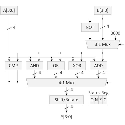
Initially, I assumed I’d be implementing a traditional architecture, something similar to the image I just whipped up below. I’ve omitted the control signals and status logic from this diagram for simplicity. Suffice it to say that the 4-bit status register comprises four flags: O (overflow), N (negative), Z (zero), and C (carry). If this diagram doesn’t make any sense to you, then may I be so bold as to suggest you look for a second-hand copy of Bebop Bytes Back: An Unconventional Guide to Computers.
A traditional 4-bit ALU (Source: Clive “Max” Maxfield)
The “0000” input of the 3:1 multiplexer allows us to pass the current value in the A register untouched (by ORing it with zeros, for example) for use with the shift and rotate instructions.
I was visualizing each of these functional blocks implemented on pieces of stripboard, with all the modules attached to a thin sheet of plywood (or something similar). Each arithmetic/logic function would have LEDs on its outputs. The multiplexers would also have LEDs on their control inputs, as well as additional LEDs to indicate which group of inputs was currently selected.
The advantage of this implementation is that it’s bog-standard, straightforward to explain, and simple to understand. The disadvantage is that it’s “so-so soup” that’s been done to death.
I was chatting with my friend Joe Farr about this just before breaking for the New Year holiday. We decided to each mull things over in our own way, with the goal of coming up with something “interesting” and “unexpected.” We set some ground rules as follows:
The ALU should be capable of supporting 16 operations: ADD, ADDC (add with carry), SUB, SUBB (subtract with borrow), AND, OR, XOR, NOT, CMP (compare), SHL (logical shift left), SHR (logical shift right), SHRA (arithmetic shift right), ROL (rotate left), ROR (rotate right), ROLC (rotate left through carry), and RORC (rotate right through carry).
The CPU will have a 4-bit data bus and a 12-bit (4K nybble/nibble) address bus. The idea is to begin by simulating both the CPU and its ALU inside the Arduino Uno. Later, the ALU can be brought out into the physical world with lots of LEDs (it’s important to remember the LEDs).
The first 256 nybbles of memory will reside in the Arduino. The first-pass goal is to create a program that requires only these 256 nybbles to generate 10 random numbers, store them in 10 memory locations, calculate the average, and store the result in an 11th location.
For more complex tasks, a cheap-and-cheerful 8-pin 24C32 4KB EEPROM device can be attached to the Arduino via I2C to provide additional memory, if required. This device is available in a breadboard-mountable PDIP package, thereby making it accessible to beginners.
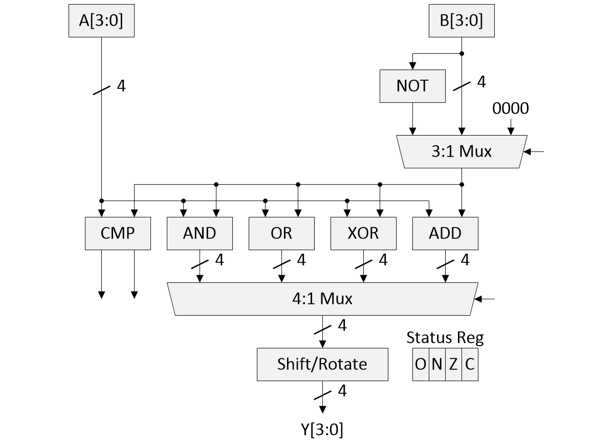
Joe and I just had a post-New Year Zoom call to share and compare our implementations. For my part, I decided to implement all 16 ALU functions as separate logic blocks, as illustrated below.
I opted to have traditional A and B registers, but to have them drive all 16 functions. Every time a new value is copied into an A or B register, all the functions are evaluated. Each of my functions has its own 4-bit data (D) result register and its own 4-bit status (S) register.
Alternative ALU implementations (Source: Clive “Max” Maxfield)
Addresses 0x000 through 0x00F in my main memory contain hard-coded literal values 0b0000 through 0b1111. My programs automatically start running from address 0x010 in the main memory.
My 16 ALU functions live in a separate address space from the main memory. They are addressed as 0x0 through 0xF.
My CPU supports only four instructions: MOVE, JUMP (unconditional jump), JUMP_IF_0 (conditional jump if the specified status bit is 0), and JUMP_IF_1 (conditional jump if the specified status bit is 1). When coded in a 4-bit nybble, these instructions look like the following:
00?? MOVE
01XX JUMP
10?? JUMP_IF_0
11?? JUMP_IF_1
In the case of a MOVE, the ?? Bits decode as follows:
00 Memory to Memory Source: 3 nybbles1 , Destination: 3 nybbles1
01 Memory to A or B Source: 3 nybbles1, Destination: 1 nybble2
10 Data to Function Source: 1 nybble3, Destination: 1 nybble4
11 Function to Memory Source: 1 nybble5, Destination: 3 nybbles1
1Address in main memory
20b0000 = A, 0b0001 = B
3This will be the 0b0000 (0) or 0b0001 (1) data value that’s written into this function’s carry (C) status bit.
4This will be the address of the function in question (from 0x0 to 0xF). The LSB of the data nybble will be written into the C (carry) bit in this function’s status register.
5This will be the address of the function in question (from 0x0 to 0xF). The value read out will be a copy of this function’s data nybble.
In the case of an unconditional JUMP_IF_0 or JUMP_IF_1 instruction, the XX bits are “don’t care” (we might find a use for them later). An unconditional JUMP instruction will be followed by 3 destination address nybbles. The program counter (PC) will be set to this address.
In the case of the conditional jump instructions, the ?? bits decode as follows:
00 = bit 0 in the specified status register
01 = bit 1 in the specified status register
10 = bit 2 in the specified status register
11 = bit 3 in the specified status register
A conditional JUMP instruction will be followed by 1 source address nybble and 3 destination address nybbles. The source address nybble will be the address of the function in question (from 0x0 to 0xF); in this case, the system will look at the status register nybble associated with the specified function. The three destination address nybbles will be the target jump address in memory if the condition associated with this jump is met.
Reading the data value from a function doesn’t affect the function’s copy of that value. Performing a conditional jump doesn’t affect the function’s local status register. A program could load values into the A and B registers and then access the outputs—both data and status (via conditional jumps)—from multiple ALU functions.
That’s all I have so far.
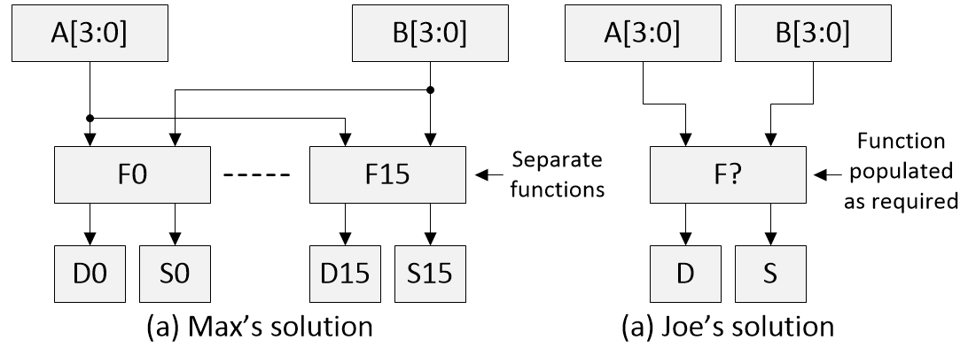
Interestingly enough, Joe also decided that addresses 0x000 through 0x00F in the main memory will contain hard-coded literal values 0b0000 through 0b1111. Furthermore, Joe also decided to support the concept of A and B registers, but after that, he went in a completely different direction.
Joe’s A and B registers, ALU_Mode, ALU_Out, and ALU_Status are all readable/writable nybbles in his main memory map. As illustrated in the image above, Joe supports only one ALU functional entity, whose mode he populates with whichever function is required at that time. That is, Joe first loads his A and B registers, and then loads his ALU_Mode, after which he can access the ensuing ALU_Data and ALU_Status values.
Another aspect of Joe’s implementation is that it supports only a single instruction: MOVE. Every MOVE instruction has an associated 3-nybble source address and a 3-nybble destination address. Furthermore, since every instruction is a MOVE, there’s no need to represent it with an opcode, which means each instruction is essentially composed only of a source and destination address.
To be honest, I’ve only skimmed the surface of Joe’s implementation, which also boasts (“flaunts” might be a better word) of two index registers and a stack, along with the ability to push data values onto the stack and pop them back off again. And then things start to get interesting.
I’m still trying to wrap my brain around all of this. I’ll report further in a future column if you are interested in my doing so. In the meantime, I’d be extremely interested to hear your thoughts on all of this. What would you do if it fell on you to create a 4-bit processor, especially if the task was to come up with an innovative and/or unusual solution without care for performance or power?


” (c) involve a lot of light-emitting diodes (LEDs).”
– That’s what it’s all about.
I know one guy who set out to build a digital computer using only the technologies available circa 1899 — specifically small neon lamps and light-dependent resistors (LDRs), which means the logic gates themselves light up — mega-cool!!!
I remember the NE-77 three-electrode neon lamp.
You might be interested in this modern equivalent.
Each gate has a forward biassed LED built into the base circuit of the transistor inverter. Not only does it provide an essential voltage hurdle, which improves noise immunity, but every gate lights up.
This hackaday project built a very small 8-bit computer using LED_Transistor_Logic
https://hackaday.io/project/169948-lcpu-a-cpu-in-led-transistor-logic-ltl
WOW! That IS tasty — Led-Transistor Logic (LTL) — who would have “thunk”?
Joe’s solution has 12 inputs: A[3..0] and B[3..0] and F[3..0], and eight outputs: D[3..0] and S[3..0]. Thus, Joe’s solution could be implemented as a lookup table in a 4096-byte read-only memory.
If the outputs of Max’s solution feed multiplexers to choose which one function’s D and S are used for any given instruction, Max’s solution and multiplexers can be implemented as a lookup table in a 4096-byte read-only memory.
Hi Peter — Remember that the status flags O, N, Z, and C are also outputs, plus the C flag can act as an input to certain functions (ADDC, SUBB, ROLC, RORC, etc.)
Yes, the ROM would be 8192 bytes to include the C input. Also, for LEDs and for teaching, the discrete gates are much better.
Working on embedded systems in 1980, we were already used to programming software into PROMs. I was tasked to build a tester to reproduce one customer’s system’s existing synchronous clocked waveforms, so another engineer could test our interface board before we had access to the customer’s system. I used a crystal oscillator driving a synchronous counter driving a PROM driving D flipflops.
We used PROMs to implement many things in the early 1980s, from gathering simple “glue logic” functions to acting as look-up tables to forming the heart of simple state machines. Ah, the good old days 🙂
It was proven that the best 4-bit ALU is SN74181.
Perhaps, it would be better to follow its inner structure.
Ah, the 74181. That was an iconic 4-bit ALU. I say was because it’s now obsolete and not actively made by major manufacturers anymore, but you can still buy them as new old stock (NOS).
It had ~70–75 gate equivalents (~170+ transistors). It boasted 32 total functions (16 logic and 16 arithmetic), but many of these were “odd” functions that fell out naturally from the internal logic after the “real” functions had been implemented.
The 181 offered a masterclass in elegant, transistor-efficient digital design. It enabled bit-slice CPU designs (e.g., 8-bit, 16-bit, 32-bit CPUs built from 4-bit slices); it was used in machines like the PDP-11, VAX, and countless minicomputers; and it taught an entire generation of engineers how ALUs really work.
But where would be the fun in simply replicating something that has been beaten (analyzed) to death? No, I think it’s better to create something innovative and different to give everyone something to argue about LOL
Anyway, designing ALU in SN7400 series needs a lot of soldering. To minimize it, the functions CMP, XOR, ADD, and negation are usually performed in a single adder by control of carry, XOR etc.
But soldering is fun LOL I’m actually thinking of the final ALU as a piece of wall art (remember each sub-function and multiplexer will be festooned with LEDs — mounted in a shadow box, doing something like calculating the value of Pi for all eternity.
Hi Max,
Looking forward to the next update on your 4-bit explorations.
Many years ago (2004) Dieter Muller wrote a great article on how to use multiplexers to build ALUs.
http://6502.org/users/dieter/a1/a1_4.htm
A 4-input mux, like a 74xx153 can generate all 16 Boolean combinations of 2 input bits.
So with four 74xx153s you can have XOR, AND, OR and all the other combinations of the A and B inputs.
Do you document any of your work on Github?
You might this Digital simulator by H. Neemann – a great way to try out logic designs – either abatact or using 74xx series packages.
https://github.com/hneemann/Digital
One Hungarian enthusiast has produced a 4-bit machine using 450 discrete transistors.
There is a Youtube here:
https://www.youtube.com/watch?v=ZgkxWni4V3E
You can set the subtitles to the language of your choice.
https://youtu.be/ZgkxWni4V3E?t=1
Personally, I like bit-serial machines, which might be slow, but in wordsizes above 8-bits, they save a huge amount of hardware.
You can have a 16-bit machine in fewer than 700 NAND gates (transistors). But that is for another post.
You are correct that the 74xx181 has been obsolete for years, and also correct that it had many “odd” functions.
The currently available 74HC283 is a 4-bit fast adder, and is a better starting point for arithmetic operations such as ADD, ADC, SUB, SUBB, CMP, INC, DEC etc.
For the shifts and rotates, the 74HC194 is a 4-bit bidirectional shift register.
However, a lot of the useful logic is wrapped up inside the ‘283, with no access to internal functions.
So I derived a 1-bit ALU (replicated 4 times) which exposes the internal signals.
It’s based around a full-adder where you have access to both the individual sum and carry outputs. We know sum is the XOR and Carry is the AND, so we can use a multiplexer to select either of those Boolean functions. The other trick is if you OR sum and carry, you get the Boolean OR.
At 10 simple gates per bit (another XOR for subtraction and another to invert the output) it would be 12 ICs on a breadboard. 13 if you include the output shift register.
You might be interested in Minimalist Computing – a Facebook Group of 15,000 members, where we discus these topics regularly.
https://www.facebook.com/groups/minimalistcomputing
This is very interesting — re the shifts and rotates, rather than a 194 shift register, I was planning on implementing them via combinatorial logic in the form of multiplexers — re the Facebook group, I’m not on Facebook, but I’m sure many other readers of this column are.
Max,
I will link your blog to all my members in Minimalist Computing.
Part of the groups’ activities is to study early, simpler machines, and find ways to implement them using readily available parts. We try to stick to a list of 60 or so 74HC parts that can still be purchased from mainstream suppliers.
As well as 74HCxx Homebrew, there is also an interest in discrete transistor machines. Low cost modern pcbs, now make these technologies and designs much more accessible.
From LED-DTL, I came up with White Light Logic. Here I replace the forward biased base LED with a white LED. White LEDs have a forwad voltage drop of at least 2.5V, and will produce visible light with as little as 6uA of current.
My basic gate is a 3-input NAND, from which you can build almost anything. Using through-hole components the 3-input NAND occupies a 10mm x 10mm pcb tile.
I produced a D-type flipflop using White light Logic, and have successfully clocked it at 12.5MHz to provide a divide by 2 output.
https://hackaday.io/project/203927-white-light-logic
We also have some very interesting 4-bit activity in the group, including a discrete transistor 4-bit machine which uses 450 transistors and about 1000 diodes.
Although not related to my current 4-bit CPU project, you might find my old HRRG Computer concept to be of interest: https://www.clivemaxfield.com/diycalculator/sp-hrrgcomp.shtml
I disagree,
the 74181 was a convenient kludge.
It is long dead – so no need to worship it anymore.
If you don’t nail your colours to its mast, you can probably come up with something much better for a lower transistor count.
How about 40 simple gates, for something that is functionally much better?
Perhaps this is vanity: I’ve done one bit and four bit processors for FPGA implementation.
The rational is at: https://github.com/jimbrake/ISA-Exploratorium/blob/main/LEM/LEM_exec_sum.pdf
(LEM stands for Logic Emulation Machine)
The FPGA resource usages are at:
https://github.com/jimbrake/ISA-Exploratorium/blob/main/_all_projects/unique_projects_251211.pdf
For the LEM series LUT counts range from 79 to 172 LUTs.
Whereas a 16-bit unique full featured processor starts at 400 LUTs.
This is very cool — thanks so much for sharing — Max
I started life on the i4004 (Intel) and it’s been ALUs and CPUs ever since, Fairchild 9400 bit-slice, 100K ECL ALU for a systolic array. So, full speed ahead, Max.
I think you architecture might lend itself to 2 very important ideas. Firstly, you can deploy more LEDs. Secondly, there is some gain to be had by doing things like using the XORs in the half-adders for your XOR block.
Are the two comparator outputs where the same value on both means equal?
If I used XOR for bit-wise comparisons will it be able to set the Z flag?
This is gonna be insanely cool!
Re: the architecture. I meant as compared to Joe’s. Joe’s multipurpose function-plexer would be a design playground, so that’s cool in its own right. So, LEDs were the tie breaker.
I’m in touch with Joe almost every day — we’re going with his implementation because it has some really cool features (like being able to switch between 8-bit and 12-bit addressing on the fly, which will make reverse engineering our code a real treat 🙂 Don’t worry, there will still be lots of LEDs!
I was chatting with Joe about the idea of creating a little program that combines address mode switching with recursion with self-modifying code — that will make your eyes water LOL
Self-modifying code, eh? My parents warned me about doing that. Well, er, I might have done it when I was trying to save memory on a MC6809; but, I didn’t inhale.
If Joe’s architecture lends itself to address mode dexterity and recursion, I’m all for it. Anything I can do to help let me know. In the meantime, I’ll follow along.
Regarding my earlier typo-laden question about the comparator outputs, I referred to Figure 8.31 in Bepop Bytes Back and later your comments below to resolve it.
Hi Doug — I’m replying to your last question here because there’s some sort of depth limit in this commenting system re replies.
You said: I have a question about the value that appears in the zeroth nybble of $00: should it be a 0 instead of a 2?” It should — I just emailed Joe about this.
“Reading the assembler I see where the first several instructions are using the literals at memory block $00 to set IX. I was assuming those first 16 nybbles are read-only, but… and a quick scan of what I could see of the code didn’t appear to ‘move’ a 2 into nybble 0 of block $00. And the move into IX displays as a 0 on the emulator.”
This is still early days — I know addresses $00 thru $0F are supposed to be hard-coded with $0 through $F — but I don’t know how they get there and I don’t know if they are read only — making them writable could add another layer to the confusion 🙂
Joe just replied: “Yea, it was 0 originally, right until the emulator started stamping all over memory lol”
If you perform any 4-bit logic operation (AND, OR, XOR), it will set the N and Z flags. If you perform a COMP (compare), it will set the O, N, Z, and C flags to represent A > B, A < B, A == B (== 0), and A == B (!= 0). The clever thing is that we have only a MOVE instruction, but it can do ADD, ADC, SUB, SUBB, AND, OR, XOR, NOT, COMP, SHL, SHR, SHRA (arithmetic shift right), ROL, ROR, ROLC (thru carry), and RORC (through carry), plus we have three 12-bit index registers/counters, a 15 nybble stack, AND we support subroutines (to a depth of 3).
Do you have any further online documentation of what you propose?
Not yet — it’s evolving as we speak — we just added the ability to select between 8-bit and 12-bit addressing. Just to add to the fun, we can switch the addressing mode under program control on the fly (that should give disassemblers a bit of a headache LOL).
Just for giggles and grins, Joe has the first pass at an emulator up and running. You can see an image here: https://www.clivemaxfield.com/wp-content/uploads/2026/01/emulator.png
Tell Joe, nice job on the emulator. Looks like a potential mock up of a front panel if I can get at those signals.
I have a question about the value that appears in the zeroth nybble of $00: should it be a 0 instead of a 2?
Reading the assembler I see where the first several instructions are using the literals at memory block $00 to set IX. I was assuming those first 16 nybbles are read-only, but… and a quick scan of what I could see of the code didn’t appear to ‘move’ a 2 into nybble 0 of block $00. And the move into IX displays as a 0 on the emulator.
Did I overlook something?