

The world has seen a ton of MEMS devices built in the last few years. Of course, MEMS technology has been around for decades, but it’s really been the ability to fabricate cheaply, coupled with high-volume applications, that has driven the more recent surge.
While MEMS devices have historically been built out of many different substances, the “fabricate cheaply” thing comes partly from the ability to use silicon – either etching the pieces out of the wafer (bulk micro-machining) or depositing films onto silicon and etching those (surface micro-machining).
I never noticed this, but it turns out that, as nice as silicon can be, there are certain kinds of mechanical interactions you don’t really see. You see bending, expansion/shrinkage, movement in proximity (like interdigitated fingers), and vibration, for instance, but we never get to see any hot silicon-on-silicon action. You know, where one part literally slides across another or rotates in contact with a surface or rubs in some other way. Largely because, well, it would be too hot. Among other problems.
So this is a story of how a team from TU Delft (the Netherlands), Argonne Labs (Illinois), and Falco Systems (also the Netherlands) came up with a material that could be used where silicon couldn’t, and that could be integrated into typical manufacturing facilities. What follows comes both from their paper and from comments from one of their team members, Anirudha Sumant.
Tribology – not the study of human clumping
The issue of surfaces rubbing or sliding has obvious implications in the macro-mechanical world. It’s why we have bushings and bearings and lubricants. Not sure that a grease zerk would work particularly well on your MEMS device, however. There’s a name for ways in which different materials deal with surface contact interactions like rubbing, and it’s my new vocabulary word for the month: one speaks of the “tribological” properties of the material. (Which is why the kind of static electricity created by, say, rubbing a balloon is referred to as tribo-electricity.)
And it turns out that silicon’s tribological properties aren’t great. Which is interesting, given the use of various silicon-based substances for lubrication. But, specific chemistry of silicones and silicas aside, the importance of tribological properties changes as you miniaturize your mechanical parts. That’s because some physical properties are related to the area and some to the volume of the piece.
In general, the kinds of issues related to area involve:
- Adhesion
- Friction
- Meniscus forces (and stiction)
- Viscous drag forces
- Surface tension
Meanwhile, issues related to volume include:
- Inertia
- Electromagnetic forces
And here’s the deal: when you go from, say, the millimeter level to the micron level, the area-related issues “reduce” by the square of the dimension, or by a factor of a million. The volume-related issues scale as the cube of the dimension, so they go down by a factor of a billion. But, flipping that around, it means that, on a relative basis, the area-related issues are now a thousand times greater than the volume-related ones at the micron level as compared to the millimeter level. Which means that these surface effects become more dominant and more important to deal with.
So, if silicon isn’t particularly good in this department, what alternatives are there? A number of different substances have been tried, but an important goal is to make sure that the selected alternative is relatively friendly for a high-volume manufacturing process. So lots of exotic materials can be eliminated immediately, and the list of remaining possibilities becomes pretty short.
- Silicon carbide (SiC) is a possibility, but it gets deposited at a temperature that’s higher than desired – in the 900-1000-°C range. Machining techniques also aren’t well established, and there are issues of doping and stress management.
- Diamond is interesting, but single-crystalline diamond takes too long to grow; you need to give the atoms time to find and settle into their lowest-energy (cubic) place in the lattice.
- Diamond-like-carbon (DLC) is an amorphous alternative with sp3 bonding that can be deposited much more quickly, since no attempt is made to grow a crystal. It has a mix of hexagonal and cubic structures. The good news is that, because there’s no lattice, it’s more flexible and can form a more conformal layer. But it’s not conformal enough to coat the kind of complex surfaces and high-aspect-ratio holes you might require in a MEMS device. Its deposition rate, while faster than growing a crystal, is still relatively slow and, critically, leaves high internal stresses.
In fact, this internal stress was the big bugaboo that had plagued many of the diamond-related projects; most people had abandoned diamond as a viable candidate. Kind of like internet dating: looked interesting in the profile, but dinner in person was more problematic.
This team came back to diamond, however, finding that doping with nitrogen and creating “nano-crystals” (rather than one big crystal) was easy to manufacture, and, importantly, it had both good electrical conductivity and bad thermal conductivity. We’ll come back to why that helps in a minute.
UNCD – not University of North Carolina, Durham
They refer to this material as “ultra-nanocrystalline diamond,” or UNCD. And it turns out to have favorable chemical, physical, and mechanical properties, a high water angle due to hydrogen atoms coating the diamond surface (which means poor wetting, which helps reduce stiction), and it can be easily integrated into a silicon fab. (Although its 850-°C deposition temperature would make it unsuitable for MEMS-last integration into a monolithic CMOS/MEMS chip.)
But, most importantly, it has good tribological properties. You can create elements that rub or move against each other, and they will not degrade prematurely. And, as a bonus, it has a higher Young’s modulus than silicon, making it stronger and allowing it to bend farther than silicon can.
UNCD has been used for structural purposes before, with a piezoelectric or other element employed for actuation, but the team wanted to prove out UNCD itself as an actuator. The main way they would make it work would be to exploit its high conductivity to run a current through an element, causing it to heat up and expand. This is also why poor thermal conductivity is important: you don’t want all that heat you’re working so hard to generate simply to be wicked away and dissipate; you want it to stick around in the place where you created it – and only in that place.
The electrical conductivity comes courtesy of the nitrogen and the boundaries of small sp2-bonded (think graphene) clusters at the grain boundaries (the insides of nanocrystals would be sp3 bonded). Resistance drops as temperature rises, as with semiconductors in general, but if you go above 600 °C, some of the sp3 bits start to react with ambient oxygen and convert to sp2 in a process called graphitization.
Deposition involves a stack that starts with a 10-nm tungsten layer, which improves uniformity. They then use “ultrasonic agitation” to deposit diamond nano-seeds onto the surface, after which they grow the layer using microwave plasma CVD (MPCVD) for 10 hours at that 850 °C until it’s 3.3 µm thick.
Critically, the atmosphere during growth contains 20% nitrogen gas. This means that the nitrogen is integrated uniformly into the substance as its grown – there’s no need to dope the diamond in a separate follow-on step using implantation, which can cause damage and requires a 1000-°C anneal, which can cause further damage.
The resulting layer is almost semi-metallic, with a measured resistivity of 136 ?cm.
Chevrons – not your neighborhood gas stations
They built a movable “shuttle” to try this out. I’ve illustrated the overall structure below. The idea is that, by running a current through the “beams” at the top, they expand and create a force downward (as drawn).
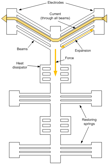
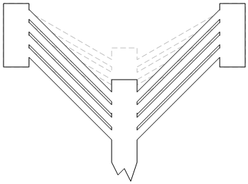
The beams are working against the springs; the more beams, the more force is available to move the shuttle. The difference between unactuated and actuated is illustrated in the next image, just to reinforce how this works. You can see the unactuated position in the dashed gray line; the black lines show the actuated position. For this to happen, those beams have to get longer. Which they do, thanks to the heat caused by the current – as much as 520 °C.
They played with a number of configurations: they needed to optimize the angle and length of the beams so that they could get as much force as possible without buckling the beams. Buckling is less of an issue with short beams, since their stiffness can resist the buckling temptation, but longer beams need more delicate care.
One element I wondered about was the uniformity of the beams. To me, having all those beams in parallel would seem like a potential issue if they weren’t well matched. If one beam were pushing harder or farther than its neighbor, it would end up dissipating energy stretching the neighboring laggard rather than pushing the shuttle forward (or, looked at another way, the slightly-shorter beam would actually be holding things back).
This reminds me of the issue of using voltage sources in parallel: you’re not supposed to do it. Why? Because that’s what the prof said in undergraduate electronics, and, at that stage of one’s career, one does not question such things; one merely absorbs and regurgitates on the exam. But, in real life, if you try to do that with voltage sources that aren’t exquisitely matched (or designed for that specific use), then you won’t get multiple voltage sources all doing their share, and funny things can happen.
Mr. Sumant confirmed, however, that beam uniformity is good, and each one of them is pulling – or, rather, pushing – its own weight.
On their larger versions, they also added a “reference” beam. They needed to be able to measure the movement of the shuttle, but they wanted to exclude noise from movements of the chip as a whole. So they used that stationary beam as a reference, subtracting out its movements from the measured shuttle movements to get a clean measurement of the shuttle’s response to actuation.
In the end, they found that they could move the shuttle as much as 1750 nm with good control using voltages up to 25 V (180 mW). They confirmed that the heat does not move through the works; the 520° temperature is reduced to 25° at the far end of the shuttle. And there’s no hysteresis in the movement (unless they heat even further, where graphitization starts).
So their take-away is that UNCD looks like a favorable material for building MEMS elements that will have one surface moving over another. Pending confirmation and commercialization, of course.
More info:
Original paper (behind paywall)


What do you think about using ultra-nano-crystalline diamond as an actuator?