How to get accurate inductance extraction for superconductor ICs
By Hossam Sarhan and Dusan Petranovic
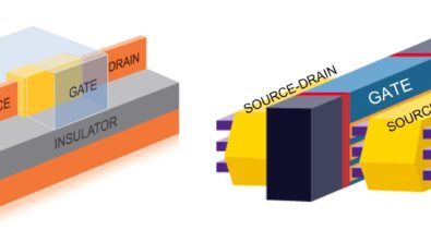
Supporting the high performance and reliability needed for artificial intelligence (AI), data centers and cloud computing requires powerful and efficient integrated circuits (ICs). More semiconductor companies are considering superconductor ICs for their unique properties that allow ultrafast processing of digital information. These properties include fast superconducting transmission lines and active devices called Josephson junctions, which generate picosecond waveforms. These junctions have low power consumption, enabling dense device integration and reducing communication delay. The fabrication technology is based on niobium, which is simpler than mainstream semiconductor technology.
However, as superconducting ICs move from universities and research labs into the industrial mainstream, designers need innovative physical verification electronic design automation (EDA) solutions to ensure the performance and reliability of these superconductor ICs. Designers need an efficient methodology to accurately extract layout parasitics, such as inductances, and enable the high-performance capabilities of superconductor ICs.
Parasitic extraction for superconductors technologies
Superconducting ICs use inductances to store and route flux quanta and single flux quantum pulses generated by Josephson junctions. Superconductor ICs also include interconnects that connect the cells. Designers must extract the parasitics of these interconnects for accurate circuit simulation. In these superconducting lines, only inductance and capacitance parasitics are extracted, as resistance is zero.
Superconducting interconnects have two types of inductances: magnetic and kinetic. Magnetic inductance depends on the current flowing through the conductor and its frequency, while kinetic inductance is a characteristic of superconductors related to the inertial mass of mobile charge carriers in alternating electric fields [1]. A change in electromotive force is opposed by the inertia of the charge carriers, similar to how a change in electromotive force is opposed by the finite rate of change of magnetic flux in an inductor. The resulting phase lag in voltage is identical for both energy storage mechanisms, making them indistinguishable in a normal circuit.
While EDA tools for magnetic inductance extraction exist in conventional IC design flows, superconductors require a methodology to extract both magnetic and kinetic inductance efficiently. One way is to use a dedicated Technology Computer-Aided Design (TCAD) solver to extract kinetic inductance. However, TCAD solvers suffer from long runtimes on big designs and full-chip scale. This highlights the need for efficient and accurate methodology for inductance extraction in superconducting ICs.
Hybrid methodology for inductance extraction
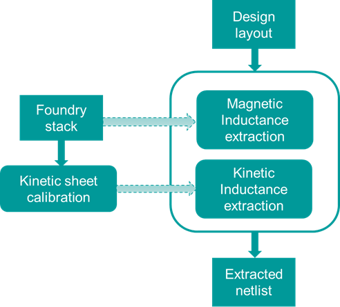
We developed an innovative hybrid methodology to extract both magnetic and kinetic inductances for superconductor designs [2]. For magnetic inductance extraction, designers can use an industrial solver engine that considers the current flow through the interconnects. For kinetic inductance, on the other hand, extraction uses a calibration mechanism based on foundry measurements. The process extracts and generates both inductances simultaneously.
The kinetic inductance can be calculated using kinetic inductance sheet values. These tables are populated using a calibration process. You can then include the resulting kinetic inductance values in the netlist along with magnetic inductance for subsequent simulations. This approach ensures a comprehensive and accurate representation of inductance in superconductor designs.
Results using industrial parasitics extraction flow
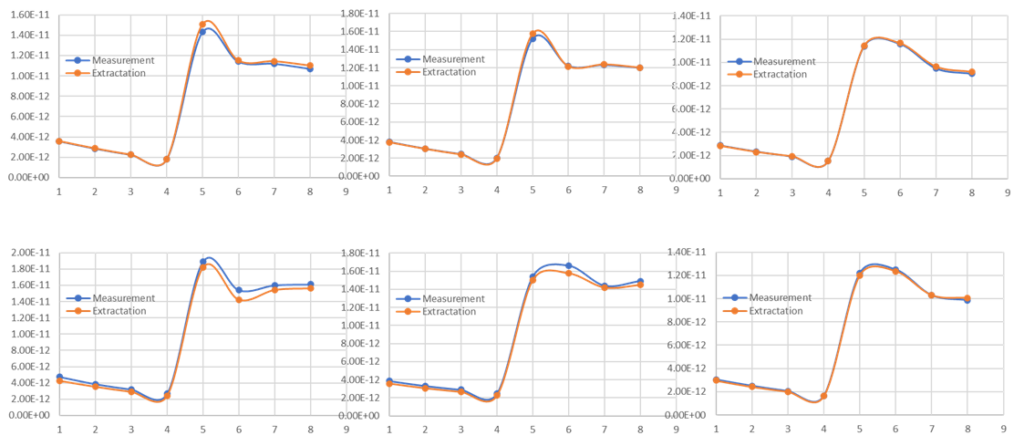
For a test case, we used the Calibre xACT [3] and Calibre xL [4] parasitic extraction tools to extract inductance in a superconductor chip of size 4970 µm x 4885 µm. The extraction process for 48 transmission lines on the chip took 125 seconds. The results showed a high correlation between the extracted total inductance and the physical measurements (figure 2). These results demonstrates that the new extraction methodology provides an efficient methodology for extracting total inductance (both kinetic and magnetic) for superconductors on a large set of test structures and on a full chip using an industrial EDA tool flow.
Summary
Superconductors are crucial for high-performance computing technologies but raises new challenges for physical verification EDA. Siemens EDA developed a novel hybrid methodology for inductance extraction in superconductor process nodes, accounting for both magnetic and kinetic inductances. This method was tested on a full chip superconductor design, resulting in highly accurate results compared to physical measurements within a short runtime. This efficient and accurate approach for inductance extraction provides a successful way to handle superconductor designs.
Acknowledgment
The authors greatly appreciate MIT Lincoln Laboratory for technical collaboration, discussions and providing reference data.
References
- S. K. Tolpygo, et al., “Inductance of Circuit Structures for MIT LL Superconductor Electronics Fabrication Process With 8 Niobium Layers,” in IEEE Transactions on Applied Superconductivity, vol. 25, no. 3, pp. 1-5, June 2015, Art no. 1100905, doi: 10.1109/TASC.2014.2369213.
- Hossam Sarhan and Dusan Petranovic, Siemens Digital Industries Software, “Hybrid methodology to extract kinetic and magnetic inductances for superconductor technologies”
- Siemens EDA, “Calibre xACT extraction.”
- Siemens EDA, “Calibre xL extraction.”