

Almost exactly four years ago, at Gigaom Structure 2014, Intel’s Diane Bryant announced that the company would be “integrating [Intel’s] industry-leading Xeon processor with a coherent FPGA in a single package, socket compatible to [the] standard Xeon E5 processor offerings.” It was a bare-bones sort of announcement with zero details, except that she expected the combination would deliver data center customers “a programmable, high performance coherent acceleration capability to turbo-charge their algorithms” and that industry benchmarks indicate that FPGA-based accelerators can deliver >10x performance gains, with an Intel-claimed 2x additional performance, thanks to a low-latency coherent interface between the FPGA and the processor.
We wrote an article at the time saying that we thought that Intel should (therefore) buy Altera. About a year later, after some high drama negotiations they did, for just north of 16 billion dollars.
Then, in 2017, Intel/Altera announced a major overhaul and integration of their tool chain for programming FPGAs for data center applications.
Software development, in our view, was (and still remains) the biggest challenge for taking advantage of the huge potential that FPGAs bring to the table for compute acceleration and (more importantly) power reduction in key data center applications. Sticking a couple of chips together in a package is nice, sure, but not too useful if nobody can figure out how to program the thing.
While all this 20x-ing and device combining sounded like a great idea, four years and over sixteen billion dollars later, there was still no evidence of the actual device Bryant had described back in 2014. We had signs in the tea leaves that such technology existed, and last month we heard that Dell and Fujitsu would be shipping servers that incorporated Arria 10 FPGAs via Intel’s Programmable Acceleration Card (which is a PCIe card that connects an Arria 10 to your processor).
But, where oh where is the actual thing – the promised package with a Xeon and (we have always presumed) an Arria FPGA connected by a low-latency coherent interface?
Finally. It’s here.
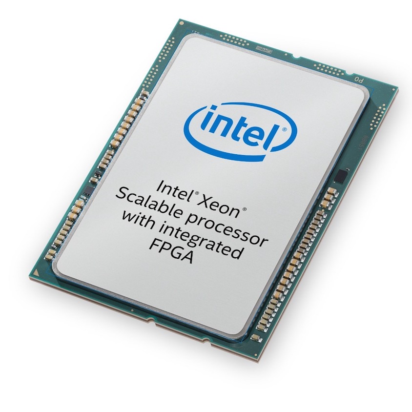
On May 18, Intel’s Jennifer Huffstetler, vice president and general manager of data center product management, announced in Intel’s itpeernetwork blog that the Intel Xeon Scalable Processor 6138P with Intel Arria 10 GX 1150 is now shipping to select customers.
Adding that “P” to the end of the part number must have taken some serious doing.
Xeon processor? Check. Arria 10 FPGA? Check. Cache-coherent interface? Intel’s Ultra Path Interconnect (UPI) provides what Huffstetler claims is “up to 160Gbps of I/O bandwidth per socket and a cache-coherent interface for tightly coupled acceleration.” She goes on to explain that UPI “allows seamless access to data regardless of where the data resides (core cache, FPGA cache, or memory) without the need for redundant data storage and direct memory access (DMA) transfers.”
The cache-coherent interface is a big deal, because it is easy to lose the benefits of FPGA-based acceleration by inefficient, high-overhead interfaces between FPGA, processor, and memory. Far too often we see FPGA implementations of key datapath elements of algorithms that run orders of magnitude faster than their software-based counterparts, only to see the benefits cancelled out completely at the system level when all the computing elements are trying to sort out data access.
Intel’s poster-child application for the new 6138P is a virtual switching reference design that uses the FPGA for infrastructure dataplane switching, allowing the processor to focus on application processing. Intel says that the solution is compatible with the Open Virtual Switch (OVS) framework and claims a 3.2X throughput improvement at half the latency and 2X more virtual machines – compared to OVS running on an equivalent processor without FPGA acceleration. This is an interesting flagship reference design for several reasons. First, it shows off only a fraction of the potential of the FPGA for accelerating specific applications and saving power. While a 3.2x advantage is formidable, there are certainly applications where orders of magnitude of improvement can be shown. But highlighting any of those applications would run the risk of painting the 6138P as a one-trick pony. Sure, it might speed up neural network inferencing by upmteen-gazillion percent, but if you’re not doing NN inferencing, why would you care?
Speaking of reference designs, what about the elephant in the room? Does the 6138P do anything to solve the core problem with FPGA acceleration – the programming model? The answer seems to be “kinda.” Let’s start with the low-hanging fruit. For numerous “killer” applications, FPGA IP can be pre-designed, packaged with reference designs, and sold as part of solutions that require zero FPGA knowledge on the part of the customer. For the mass server market, that will be the first line of defense against the programmability problem. Expect to see a lot of third parties developing software/hardware IP that attacks common applications in 5G network processing, artificial intelligence, data and video analytics, and machine learning – with carefully-optimized FPGA acceleration strategies posting some impressive results with the 6138P.
The very existence of the 6138P simplifies the delivery of such IP dramatically because it provides a standardized platform and architecture to develop against. It is extremely challenging to develop “generic” IP for processors and FPGAs working together that is independent of the particulars of the processor, the FPGA, and the interconnect schema. By providing a stable, concrete platform, Intel opens the door for widespread third-party development. Intel calls this sort of pre-developed IP “drop-in” solutions, and they’ve created a portal to catalog third-party offerings in segments such as artificial intelligence, genomic sequencing, cybersecurity, video, networking, and financial analysis.
For applications that cannot be addressed with off-the-shelf IP and reference designs, Intel has done a good job with their first-round development environment. The Intel “Acceleration Stack for Intel Xeon CPU with FPGAs” consists of software, firmware, and tools designed to “make it easier to develop and deploy Intel FPGAs for workload optimization in the data center.” The acceleration stack includes hardware interfaces and associated software APIs for interfacing Xeon processors to FPGAs.
We say this is a “first step” because the task of making FPGA-based acceleration available to the mainstream is still a daunting one. The number of actual FPGA experts in the world is vanishingly small, and there is an enormous barrier in equipping and educating even the most talented software developers to create optimized FPGA-accelerated applications. Want a taste of the depth of the lack of understanding? Check out the discussion on Hacker News about this very announcement. I know, one should never read the comments, but this is a group primarily made up of talented software engineers trying to make sense of this whole “FPGA thing.” The amount of confusion, misinformation, and misunderstanding is sobering.
There are a variety of options built into (and usable with) Intel’s acceleration stack for targeting the FPGA portion of the processing engine. If you’ve got FPGA experts on the team, plain-old RTL design (with synthesis and place-and-route) gives the most control over optimization and the most flexibility in the architecture of the design. Intel also now offers high-level synthesis (HLS) technology, which is really a power tool for hardware engineers rather than a tool to allow hardware implementation by software engineers. HLS particularly shines in data flow designs such as DSP, video processing, and similar problems – providing a quick way to explore parallelism, pipelining, and alternative microarchitectures, taking advantage of the rich arithmetic resources on today’s FPGAs (hundreds to thousands of hardware multiply-accumulate units). For the more software-centric, Intel (and formerly Altera) has long supported an OpenCL flow that does a reportedly respectable job taking GPU-style code and delivering FPGA implementations. Other third parties support various other design entry flows aimed at various engineer demographics. Mathworks, for example, has a full suite of “Model-based design” tools that allow FPGA accelerators to be developed for a range of applications via drag-and-drop blocks in MATLAB and Simulink.
Huffstetler also gave us a look into Intel’s future plans as well, saying the company will introduce a discrete FPGA solution with faster coherent and increased high-bandwidth interconnect which will support code migration from the 6138P as well as the Intel Programmable Acceleration Card. We translate that to mean that there will be application portability to servers using Intel’s high-end Stratix 10 FPGAs in addition to the Arria FPGAs in the other two configurations.
Competitively, this development puts still more distance between Intel and Xilinx. For decades, Altera (now Intel PSG) carried on an intense rivalry with Xilinx, with Xilinx maintaining a steady market share lead in FPGAs over Altera. Now, however, the rivalry has taken a strange turn. With the acquisition, Altera – (now renamedn “Intel PSG”) understandably shifted to an increased focus on the data center – one of Intel’s most important businesses. Recently, Xilinx says they have shifted their strategic priority to data center as well, allowing the game to move from the FPGA market (where Xilinx was undisputed leader) to the data center market (where Intel has a dominant share.) Playing the other team’s game on their own home field is almost never a good idea, so we’ll see what happens there.
Early on, Intel appears to be winning. Why? By and large, most data center customers buy servers, not chips. With this announcement, Intel says Fujitsu plans to offer servers with these devices built in. We already discussed that Dell and Fujitsu are delivering (or planning to deliver) systems with the Intel Programmable Acceleration Card built in. We assume that more of the Intel partner ecosystem is spinning up to deliver systems with Intel FPGAs as well, and Intel is now touting portability of applications across the whole line, and even to systems built with discrete FPGAs (which we are assuming to include their flagship Stratix 10). While Intel is already focused on selling servers, Xilinx is trying to sell chips.
Strategically, the two companies are taking very different tacks with respect to acceleration, and Intel’s position may be hard for Xilinx to crack. Xilinx is throwing everything at the high end, working on a next-generation data center acceleration chip (dubbed ACAP – due sometime in 2019), which puts everything and the kitchen sink into giant programmable devices aimed at acceleration. Meanwhile, Intel is going broad, attacking the wider data center market with their (much lower cost) mid-range Arria FPGAs as accelerators. With Intel’s de-facto standard Xeon processors now available with FPGA acceleration build right into the package, and with planned portability to higher-end FPGA accelerators in the future, it’s hard to see how Xilinx will make the argument for designing a third-party FPGA into the Intel-owned server ecosystem. It will be interesting to watch.


