

Let’s face it: We’re addicted to SRAM. It’s big, it’s power-hungry, but it’s fast. And no matter how much we complain about it, we still use it. Because we don’t have anything better in the mainstream yet.
We’ve looked at attempts to improve conventional SRAM. We’ve looked at completely different memory technologies that might be in line to replace SRAM, like RRAM (first more than five years ago, then last year – and we’re still working on it) and MRAM. And, a couple of years ago, we looked at one attempt to create a new SRAM technology out of conventional transistors – to be clear, just one such transistor (instead of six), plus a possible select transistor.
The company was Zeno, and they were even leveraging this idea as a way to provide greater drive in a transistor – possibly meaning one could stick with older technologies for longer. But, back in the memory story, there was at least one unknown – granted, a “we think so,” but without proof.
Here’s the thing: the original technology was proven on 28-nm planar technology. Could it be leveraged onto more aggressive nodes – ones with FinFETs? While Zeno thought it should work, they hadn’t run the experiments yet to prove it.
And it turns out that there was another nagging question – one of the little details that can sabotage a great new idea. The technology was originally implemented with a buried N-well below the transistor. This wasn’t – and isn’t – part of a standard CMOS flow. Yeah, it’s possible to change flows over time, but it’s super hard, and there better be a dang good payoff from it. Is a 1T SRAM cell enough to motivate that? Perhaps, but the other question to ask – and the one that Zeno asked – is, “Is that modification to the flow really necessary? What happens if we omit the buried N well. Will it still work?”
At this year’s IEDM, they came back and reported on those two items – both in a discussion and in a paper that they presented. And the answer to the two questions is: Yes.
The next figure shows the layout at 14 nm, with a 6T conventional SRAM on the left and their 1T version on the right.
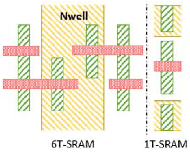
(Image courtesy IEDM/Zeno)
They also showed the “profile” at 14 nm as compared to the original 28-nm planar version. Note both the use of a FinFET and the absence of the underlying n-well on the right. This latest rendition uses the standard foundry CMOS process.
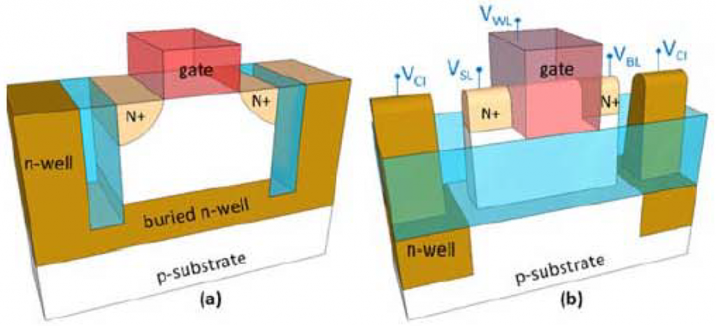
(Image courtesy IEDM/Zeno)
They presented data showing the stability of the bistable element as data is read repeatedly, showing it sticks around – and that the read operation isn’t destructive.
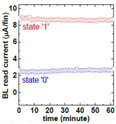
(Image courtesy IEDM/Zeno)
And they presented lots more detail on reading and writing results in their paper. If you have access to the IEDM proceedings, look for, “A Bi-stable 1- /2-Transistor SRAM in 14 nm FinFET Technology for High Density / High Performance Embedded Applications.”
More info:


I am also starting to learn about motors, but it seems a bit difficult. Hope I can stick to it. http://metonec.com/
GbE (10/100/1000Base-T) PHY IP Cores with matching 1G Ethernet MAC, PCS and TSN MAC Controller IP Cores for all your high-speed Ethernet Networking applications is available for immediate licensing.
In addition to its comprehensive digital marketing training in Jaipur, Infonic Training and Development Center offers a range of support services to help students achieve their goals. These services include career counseling, placement assistance, and ongoing support after graduation. The placement assistance program connects students with top companies in the digital marketing industry, providing them with job opportunities and a pathway to success.