

Honeywell recently released a new AMR (anisotropic magneto-resistive) sensor. We looked at this basic technology some time back, but there was another aspect of the release that confused me: the sensor was compared to a reed switch. And, at first glance, I don’t see a switch (=actuator) and a sensor as being the same thing.
For those of you steeped in this technology, what follows may seem rather basic and even obvious. But if you’re new to the space, then there’s some room to untangle some concepts that can be easily conflated.
Part of the issue has to do with being precise with terms that might be confused. If I think sloppily, I end up confusing a reed switch with a reed relay. What’s the difference? Well, a reed switch is simply a two-lead component. The switch connects the leads, presumably completing some circuit. That switch is actuated by a magnetic field (either to open or close it). That field is applied externally; exactly how depends on the application. Critically, there’s no magnetic component built into the switch.
So, in a way, the reed switch is a magnetic field detector. When the field exceeds a threshold, the reed moves, and you can think of this as a crude digital magnetic field sensor.
Now, if you include a magnetic coil along with the reed switch, adding two new leads, now you have a reed relay. This is much more of an actuator than a sensor, since it creates its own magnetic field. So switch and relay confusion can create sensor and actuator confusion.
Now let’s look at the AMR sensor schematic from the data sheet. From the outside, it may look just like a Hall Effect sensor, another sensor based on magnetic phenomena. (The field directions are apparently different, but I won’t dwell on that.)
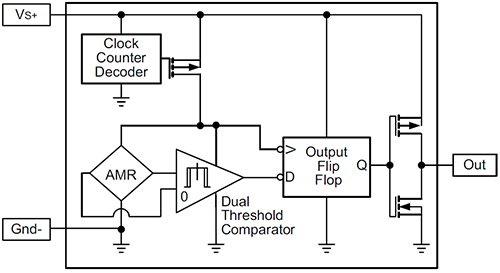
On the left is the detector circuit. Because this constantly draws power, it must do so exceedingly sparingly. The original application for this (more on that in a moment) required no more than 500 nA; Honeywell has a couple of devices, one at 310 nA, the other at 360 nA. They claim this to be more than an order of magnitude more miserly than the lowest-power Hall Effect device, with greater sensitivity.
Once it detects the field, it flips the flop and the output value changes. Now… this output looks something like a beefy CMOS output, not like a wire in a reed switch. And if it drives a CMOS input, then this will simply look like a digital indicator with no DC load current. But if the output drives something that pulls current, then the pull-up (or the pull-down) acts as a switch that makes or breaks that circuit. In this way it more resembles a reed switch.
Here’s one other possible source of significant confusion: this is not like the magnetometer you may have in your phone. Your phone mag, like most sensors, provides continuous readings of the ambient magnetic environment. The phone can go in and interrogate the value at any time. By contrast, this AMR sensor is digital: either on or off. You can’t go in and measure the actual field. So it’s unlike many other sensors out there. That on/off characteristic is what makes it appear to be a switch – and contributes to the sensor/switch confusion.
So if you think of a reed switch as a switch that can be used as a sensor, then here you have a mag sensor that can be used as a switch.
By the way, that application I alluded to above? Apparently people were trying to monkey with electric meters using magnets to disrupt the metering. So AMR sensors (it takes two of them) are used to detect such anomalous magnets. Obviously, being in a meter, they have access to power, but it’s the power someone else is paying for, so it has to be tiny so as to be undetectable on their bill.
You can read more about Honeywell’s part in their release.


