

Silicon chips and the packages that house them have been steadily drawing closer to each other over the years. There are so many pins on individual dice now – and multiple dice are going into single packages. Optimizing which bumps from which dice go to which pins is a non-trivial project.
Part of the problem is that package design and die design have traditionally belonged to different departments using completely different tools that don’t talk to each other. That’s left engineers using Excel and such to try to visualize and plan pinouts.
The bulk of this isn’t changing – there is, as far as I know, no ubertool coming that includes both silicon and package design. But what can change is the means of planning the pinout – going to something more robust and efficient than Excel.
The same problem exists, by the way, with board design. Obviously, production board design is a process completely independent of die design; the die is designed once and then used on any number of boards. But optimizing board routing can also be challenging. Not to mention that doing some trial PCB layouts when planning the die isn’t a bad idea either.
Making this easier is the goal of Cadence’s new OrbitIO tool. It allows visualization and planning of signals. Because it couches its results as routing instructions and constraints, it’s a more dynamic way of planning; changes can be made with less work.
Once planned in OrbitIO, the results get pushed down into silicon design tools – Encounter or Virtuoso – in the form of a LEF/DEF die abstract file and to their multi-die package design tool, SiP-XL, via package data. They also get pushed to Allegro PCB on the board side, meaning that the die pinout’s effect can be evaluated all the way through to trial PCB layouts.
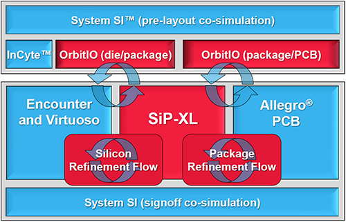
Image courtesy Cadence
In terms of evaluating what a “good” layout is, that’s partly visual, but the tool also provides lengths and number of routing layers as figures of merit. Note, however, that this analysis only goes as far as the pad ring on the die. Once planned, the effects of the pinout can be analyzed in the silicon design tool based on the data pushed to the tool by OrbitIO.
OrbitIO can be used most effectively if done prior to die floorplanning – it becomes an input to that floorplanning process. By handing data back and forth, the tools eliminate some of the tedious and error-prone steps that have to be taken with Excel and other hacks. Then pinout helps drive routing internally.
For multi-die packages, OrbitIO can work with dice in design, where pinouts can theoretically still be moved about, or with fixed dice – say, for a memory chip that’s being included in the package. The memory chip has no flexibility – it is what it is, so the tool needs to accommodate that.
If pinout is planned or changed after much of the die layout is in place, then the silicon tool can help evaluate the impact of the pinout on the die layout, and iteration is likely to find the best compromises.
You can find out more in Cadence’s announcement.


