Yesterday we looked at number of different ways of inspecting wafers. Such inspections can be an important part of a process that turns out high yields of high-quality chips. They serve a couple of roles in this regard.
The most obvious is that you catch faulty material early. If rework is possible, you can then rework it; if not, well, you don’t throw good processing money after bad.
But the other reason is probably more important: by looking at wafers at various monitoring points, you get a sense of how the equipment is working. The wafer results act as a proxy for machine monitoring.
So… what if you could measure the machine directly?
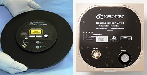
That’s what CyberOptics is doing using an in-situ approach that they say is complementary to wafer inspection. They create “fake” wafers outfitted with sensors and feed them into the equipment. The equipment thinks they’re normal wafers and processes them; the sensors measure selected aspects of the setup and report back wirelessly in real time.
And they claim to be the only ones that have this real-time capability. They say other approaches require manual “timestamping” of data that’s downloaded and analyzed after the processing is over. The Bluetooth connection to a nearby rolling host computer allows the data to be transmitted as its captured.
They have setups for measuring air particles; for leveling; gap measurement (used with thin-film deposition, sputtering, etc.); vibration measurement; and a “teaching” system that improves alignment.
Most recently they’ve announced new air particulate measurement platforms: a reticle version, which replaces not the wafer but the reticle in a lithography tool, and a smaller wafer version – 150 mm (6”, roughly). That last one might seem odd, since they say they’ve already got a 450-mm version, and bigger ones usually come later. But in this case, they had to reduce the size of the sensing and electronics to fit the smaller form factor.
Images courtesy CyberOptics
You can read more in their announcement.