

Imec has been working 2,5D IC issues with a particular focus on optimizing costs and, in particular, test yields. Yields can take what might have been straightforward-looking cost numbers and make things not so clear.
In their work on interposers, Eric Beyne took a look at three different ways of routing the signals from a wide-I/O memory. These puppies have lots of connections – like, 1200 per chip. He explored three different ways of implementing the interposer to find out which had the best cost outlook. The idea was to connect two such interfaces, with four banks of 128 I/Os each. Each channel had 6 rows of 50 microbumps. Microbump pitch along a row was 40 µm; along a column it was 50 µm. The two simply needed to talk to each other on the interposer.
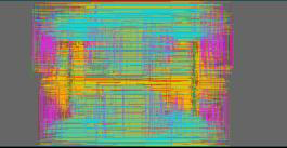
The cheapest, most traditional approach is to use PCB (or PWB) technology. An aggressive version would have 20-µm pitch and 15-µm vias. This approach resulted in an 8-layer board; you can see the layout below – lots of routing all over the place. Wire lengths were, on average, 180% of the die spacing.
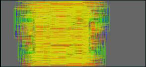
Next was a semi-additive copper process – more aggressive dimensions and more expensive. Line pitch was 10 µm; vias were 7 µm. the tighter routing allowed connectivity with only 4 layers, and the average wire length was 166% of the die spacing. You can see the slightly less colorful result below.
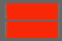
Finally, they took an expensive approach: damascene metal lines. Moving from the PCB fab to the silicon fab. But this got them down to 2-µm pitch with 1-µm vias, and that was enough to run wires straight across on 2 layers with no extra routing. In other words, wire lengths were equal to the die spacing. You can see this on the following picture.
So what happens to the overall cost? The last one is nice, but expensive to build. And here is where yield comes in. Because the “most expensive” option uses only two layers, it has the best yield. And that yield more than compensates for the expensive processing, yielding the cheapest option.
They didn’t give out specific cost numbers (they typically reserve those for their participants), but the net result is that they believe the damascene approach to be the most effective.
Images courtesy Imec.


