


Thunder is good, thunder is impressive; but it is lightning that does the work. – Mark Twain
With all the media hype and heavy emphasis on the leading-edge semiconductor process technologies that will soon reach single-digit nanometer numbers, working-class process technologies often get no respect. That’s why I was so pleased to learn that GlobalFoundries announced at the end of May that the Ultra High Voltage (UHV) variant of its 180nm ASIC semiconductor process technology—the Process Geometry Formerly Known as 0.18 micron—includes transistors capable of withstanding 700V.
Processors made with 10nm process geometries and smaller are great for crunching numbers or for impersonating HAL 9000 computers in cloud form, but when you need to drive a multi-horsepower motor or a really big solenoid actuator or deal with any sort of electrical energy straight out of a spigot connected to the AC electrical transmission system, you can’t use those teeny tiny transistors directly. They’re too fragile. They’ll go bang and all you’ll end up with is some nicely toasted silicon with the magic blue/black smoke lazily wafting away on the breeze like Robin Williams playing Aladdin’s genie, finally released from the close confines of its magic-lamp IC package.
Although 180nm technology might be considered “mature,” it still packs a wallop when it comes to handling high voltages.
We’ve Got the Power
Nearly everything electronic eventually runs on AC power. Even devices that run on rechargeable batteries need recharging. Eventually, nearly all of these devices will be plugged into the wall to sip on that sweet, invigorating electronic nectar from the AC powerline.
Worldwide, the maximum AC line voltage is 265V, so if you want to design a mains-powered power supply with a globally universal input, you need to design for that 265V line voltage. However, you don’t stop at 265V. For switched-mode power supplies (SMPS), the first thing that the line voltage encounters is a bridge rectifier and a smoothing capacitor to turn that easily transmittable AC (thank you Nikola Tesla and George Westinghouse) into DC (wily ol’ Tom Edison was right all along!). The DC rectification and smoothing puts the rectified-and-filtered DC voltage on the smoothing cap at just a hair under 375V.
You’re still not done.
For a flyback-architecture SMPS (see Figure 1), the flyback transformer reflects the SMPS’s output voltage back to the primary side, so you need to add as much as 150V for that—bringing the total withstand voltage to as much as 525V. Then there’s the spike from parasitic inductance (another 100V) to deal with, plus some design safety margin, and you can see that any SMPS control IC might need to withstand 650V.
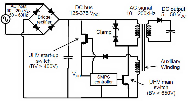
Figure 1: A simplified flyback SMPS circuit. (see Ref 1)
And that’s how GlobalFoundries’ 180nm UHV process technology got a 700V withstand rating.
Figure 2 shows a simplified SMPS block diagram with its most basic functions, which include an oscillator (everything digital needs an oscillator to make things go); some control logic; a PWM circuit that serves as the main drive to the main, high-power UHV switching transistor (which will likely need to be a discrete power device); a buffer to drive the main UHV switching transistor; sense circuitry to monitor current through the main UHV switching transistor; and an internal, line-side power supply for the SMPS controller chip.
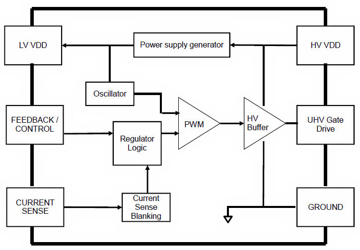
Figure 2: Simplified SMPS Block Diagram (see Ref 1)
It’s also a great idea to add some protection features to the SMPS controller chip because switched-mode supplies love to go bang, what with all that energy they’re converting from AC to DC. Typical SMPS protection features include OVP (over-voltage protection), UVLO (under-voltage lock out), OTP (over-temperature protection), open- and short-circuit protection, automatic restart, and soft start.
Most AC/DC SMPS controller ICs designed heretofore rely on analog design techniques and inexpensive, archaic process geometries (like half-micron!). Consequently, they’ve incorporated few digital functions to date. There’s been little emphasis on shrinking the digital devices on these chips, because the voltages involved are not compatible with small-geometry semiconductor processes. However, the need for more on-chip digital control circuitry grows with increased power-efficiency and safety demands.
Like everything else electronic, even power supplies are increasingly digital.
SMPS controller ICs are not the sole target for GlobalFoundries’ 180nm UHV process. Other markets that need to put more chocolate in their peanut butter—er, digital in their high-voltage analog—include applications as diverse as electric vehicles, industrial motor control, wireless charging, LED backlights for computer monitors and televisions, and solid-state lighting.
Note something especially important here: these are all growing markets for high-voltage semiconductors.
A Thoroughly Modern Process
In sharp contrast to half-micron behemoths, SMPS controller chips made using a high-voltage, 180nm semiconductor process technology seems downright sleek and modern. And, in fact, they are. While you can fit roughly 8K gates per square mm on a piece of silicon made with half-micron design rules, you get 70K gates per square mm when using 180nm design rules. That’s an 8.75x increase in device density. Where digital circuitry might have been a scarce resource on the old stuff, you can do some decidedly advanced things in GlobalFoundries’ 180nm UHC ASIC silicon. For example, a minimal 32-bit Arm Cortex-M0+ microprocessor core implementation requires only about 12K gates. (But don’t forget you’ll also need to include on-chip RAM and ROM.)
GlobalFoundries developed its UHV 180nm process technology starting with 3.3V CMOS front-end design rules. It then added back-end design rules to allow the addition of high-voltage transistors in multiple flavors. The UHV 180nm process technology uses different gate-oxide thicknesses for low-voltage and high-voltage CMOS transistors, as shown in Figure 3.
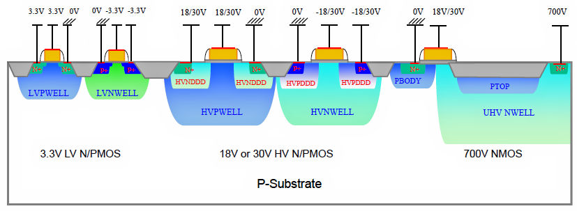
Figure 3: GlobalFoundries’ 180nm process technology permits the inclusion of 3.3V CMOS, 18V or 30V CMOS, and 700V NMOS transistors on one monolithic chip (see Ref 1)
Deeper N-type and P-type well depths, double-diffused drains, and two different gate-oxide thicknesses (you might see them in Figure 3 if you look really hard) allow the construction of either 18V or 30V high-voltage CMOS transistors on the same silicon as the 3.3V low-voltage CMOS transistors. Then there’s the 700V UHV transistor, which is formed with an even deeper N-type well and a P-type surface layer.
The result is a modular process technology architecture that can produce three distinct CMOS power-IC chip families—18V, 30V, and 700V UHV—as shown in Figure 4.
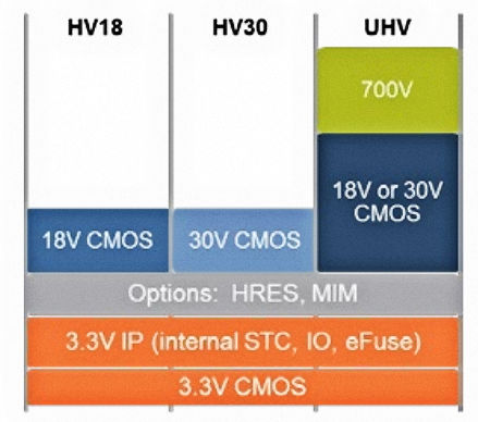
Figure 4: GlobalFoundries’ modular UHV 180nm ASIC process technology architecture can produce three distinct, high-voltage CMOS device types: 18V, 30V, and UHV 700V (Source: GlobalFoundries)
All of this exotic, high-voltage CMOS technology at 180nm has a decidedly real purpose: to add digital features to traditionally analog power ICs while reducing system costs in a variety of power-oriented applications. Combining 18V, 30V, and 700V transistors with 3.3V CMOS logic on one monolithic device eliminates the need for specifying, inventorying, soldering, inspecting, and testing discrete transistors on cost-sensitive boards.
For many who are blinded by the bright light of 7nm goodness accompanying the most advanced production processes, maybe 180nm high-voltage silicon isn’t all that exciting. But it’s sure going to be darn useful for creating a lot of very interesting and essential end products that people want.
Reference:
Don Disney, et al, “180nm HVIC Technology for Digital AC/DC Power Conversion,” Proceedings of The 29th International Symposium on Power Semiconductor Devices & ICs, Sapporo, Japan, 2017, pp. 287-290.


2 thoughts on “Zap! Zap! Zap! GlobalFoundries’ UHV 180nm Process Hits 700V”