


This week, Xilinx hit us with a duo of SerDes-related announcements – a demonstration of 112G PAM4 electrical signaling technology for optical networks, and the addition of 58G PAM4 transceivers to some of their 16nm Virtex® UltraScale+™ devices. The announcements were made at the Optical Fiber Communication Conference and Expo (OFC 2018), where Xilinx demonstrated what they claim are the industry’s first 112G PAM4 transceivers. (We think they mean “first FPGA devices with 112 Gbps transceivers,” as other companies have certainly already demonstrated SerDes at those speeds.) While 112 Gbps is definitely mind-bogglingly impressive, we won’t be seeing it in production FPGAs for awhile. The company claims that we “can expect programmable devices with 112G transceivers in Xilinx’s upcoming 7nm portfolio.”
However, this duo of announcements shines a little light on some serious challenges facing the leading FPGA company moving forward. Xilinx has spent the past several years telling us all that they are “A Generation Ahead” (meaning, of course, having about a two-year, one-process-node technology lead over archrival Intel/Altera). The primary basis for this claim (in recent months, at least) has been the delivery of the UltraScale+ families of FPGAs and SOC/FPGAs (Virtex and Zynq) – based on TSMC’s 16nm FinFET technology – WELL ahead of Intel’s delivery of their first FinFET-having FPGAs (Stratix 10 series) – based on Intel’s 14nm FinFET (previously called Tri-Gate) process.
Sounds reasonable enough, right?
To be fair, it stands to reason that Altera would lose some steam during the massive chaos that always surrounds an acquisition the size and complexity of Intel’s 2015 $16.7B buyout of the #2-ranked FPGA supplier. As one would expect, org charts were re-drawn, company cultures collided, schedules slipped, and seismic reverberations were felt throughout both Altera and Intel for months. It was not difficult to make a case that Xilinx had taken advantage of that disruption to build a significant competitive technology lead.
Lately, though, Xilinx seems to have voluntarily placed themselves in a penalty box of their own. The company has suffered a serious bout of political infighting, re-orgs, RIFs, and general chaos at the corporate level, accompanied by weeks-to-months of near-silence in PR, and culminating with a new CEO (Victor Peng) taking the helm. All of this, of course, giving Intel an all-too-welcome opportunity to make up some major ground on their primary programmable logic competitor.
Now, it looks like that “Generation Ahead” rhetoric is under some serious siege, and things in the FPGA world may get interesting quickly. In fact, one could even argue that the lead has now changed hands in several key areas. Yes, Xilinx still maintains a solid market share advantage, and we haven’t yet seen any sign of that abating. However, taking this announcement as a case in point – Intel announced recently that their first FPGAs with 58 Gbps PAM4 transceivers are already shipping. Xilinx’s response to when their 58G devices will ship? “In 2018.”
Now, If you’re not fluent in FPGA-PR speak, a little translation may be in order. “Shipping In 2018” generally means that sometime before midnight on December 31, 2018, someone with a briefcase containing a working sample of the so-claimed device will get on a plane and take it to a designated customer site. “There. We shipped.” OK, maybe that’s not the exact scenario, but you get the idea. Regardless, it sounds like maybe Intel has a few-month lead on this one.
Looking under the hood a bit on the Xilinx 58G announcement (and comparing and contrasting with Intel’s), Xilinx is adding two new devices to the Virtex UltraScale+ portfolio – the VU27P and the VU29P – with 32 and 48 of the new PAM4 transceivers respectively. By comparison, Intel’s 58G Stratix 10 TX offering packs up to 60 channels at 58 Gpbs (144 transceivers total), giving Intel a big advantage on total PAM4 transceiver count. Intel’s Stratix 10 TX family includes four new devices with 58G PAM4, and their MX family has two more, for a total of six devices versus Xilinx’s two, giving Intel more total options as well. Furthermore, Intel’s MX line has the intriguing combination of both 58G SerDes and HBM2 memory which will be a killer combination for certain applications.
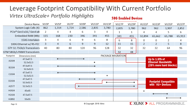
Xilinx appears (on the surface) to get the nod in terms of 58G on larger FPGAs, with “System Logic Cell” counts of 2.8M and 3.8M, while Intel’s PAM4 lineup ranges from 1.6M-2.7M “LEs.” But, hang on – what gives here, and what, exactly, is a “System Logic Cell” (anybody remember “System Gates?”) Here’s the deal: Xilinx’s primary logic structures – “CLBs” each contain eight 6-input LUTs. In the old days, Xilinx used a unit called “equivalent logic cells” which was supposed to represent the equivalent number of 4-input LUTs represented by their newer, larger, LUT6 cells. The multiplier for LUT6 vs LUT4 was 1.6, so Xilinx was claiming that it took 1.6 LUT4s to make one LUT6. Not too much of a stretch.
However, Altera did a similar adjustment with their “ALMs” (which are kinda-sorta 7 or 8 input LUTs, depending how you figure it) and decided that one of their ALMs was equal to 2.95 LUT4s (a ratio that, they have always assured us, is “conservative” relative to “competing FPGAs”). Back in Xilinx marketing land, of course, this outrage could not stand. So, Xilinx recalculated the value of their 6-input LUT to now be… (insert random boolean differential equations here, some hand waving about carry chains, muxed inputs, and DeMorgan-Freeman equivalents) … about 2.18 LUT4s per LUT6. Yep, they just brazenly upped the ratio from 1.6 to 2.18 for no reason other than, well, to make their data sheets look better compared to Altera’s. Welcome to the exciting world of FPGA marketing.
These two new Xilinx devices will be footprint-compatible with existing VU9P-VU13P FPGAs (A2577 and D2104 footprints), allowing smooth migration of backplanes and other applications from current ~28G NRZ operation to ~58G PAM4 operation over the same connectors, cables, PCB traces, packages, and so forth. PAM4 uses four logic levels rather than two, allowing twice the bandwidth at the same frequencies, thus helping the signal integrity equation significantly, compared with the usual “double the frequency” approach. The two companies are essentially at parity with this feature.
Less obvious and somewhat more intriguing is the varied approach used to create these devices. Xilinx says that their new PAM4 devices are monolithic (yep, we double-checked), meaning that the transceivers are fabricated on the same die with the FPGA fabric (and therefore, of course, using the same process). Intel is using proprietary multi-die packaging technology (dubbed EMIB for “embedded multi-die interconnect bridge”) to mate their 58G transceivers (and HBM memory as well) to FPGA chiplets fabricated with a different process. In fact, Intel’s Stratix 10 MX devices may contain chiplets from three different semiconductor vendors in the same package. Weird.
This presents a really interesting plot twist in the competitive scenario. In a previous generation, Xilinx used multi-die packaging to connect transceivers to FPGA fabric via a silicon interposer, and it was Altera singing the praises of the monolithic approach. Now, the two have changed sides (with nary a mention of that fact, of course). It seems Xilinx had a bad experience with their heterogeneous interposer strategy, and they resolved to go back to monolithic transceivers for the time being. It is possible that Intel’s EMIB is a better platform for heterogeneous integration than a silicon interposer, or that Xilinx’s past difficulties also lie in Intel’s path. It’s difficult to tell which at this point. But, Xilinx’s monolithic chips should certainly be less expensive.
Heightening the drama even more – when asked to differentiate their new 58G devices from Intel/Altera’s, Xilinx replied that their devices are “built on products that are production proven and that have already saturated these markets.” The first part of this claim – “production proven” – is just plain odd. Intel’s devices are already shipping, and Xilinx’s (as mentioned earlier) are scheduled to ship “in 2018.” Further, since Xilinx’s devices are monolithic, they are certainly all-new silicon whereas Intel’s are existing Stratix 10 FPGA chiplets mated to new transceivers via EMIB. And, historically, some of Xilinx’s worst disasters shipping new FPGA silicon have been related to transceiver problems. So, all-in-all, the “production proven” argument doesn’t pass our smell test. Xilinx does make a reasonable point that their other Virtex UltraScale+ devices have been shipping much longer than Intel/Altera’s, and they certainly have gobbled up a decent chunk of market share, but we wouldn’t say that market is anywhere near “saturated.” If Xilinx is convinced the market is saturated, one has to wonder why they are now introducing new chips for it.
Moving back to the 112G side of this announcement, we see another competitive curveball waiting in the wings. Xilinx is talking about a 7nm portfolio on the way (and has announced that they are “skipping 10nm”), while Intel has previously disclosed some details of what they call “Falcon Mesa” 10nm FPGAs. Does this mean that Xilinx is now working a “Generation Ahead” of Altera on their next launch?
Well, no.
Process node names, it turns out, have become a bit unreliable when crossing vendors. In fact Bryon Moyer discussed this issue in EE Journal just yesterday. A year ago, Intel engaged in a little creative marketing of their own, claiming that they were 3 years ahead of other semiconductor companies, despite the similar-sounding node names bantered about by TSMC, GLOBALFOUNDRIES, and others. Marketing aside, though, most analysts agree that Intel’s upcoming 10nm node will be almost identical to TSMC’s “7nm” process in density and performance, and that Intel’s 14nm FinFET (the current production node for their FPGAs) is notably ahead of TSMC’s 16nm FinFET process (Xilinx’s current FPGA production node). The real lesson here is that divining which vendor is or is not a “generation ahead” or behind requires much more analysis than simply comparing process node names. (But we’re happy to help you with that.)
Overall, we are excited to see what direction Xilinx takes under the new leadership of Victor Peng. While things appear to have gotten off to a rocky start, the technical team at Xilinx has proven themselves for a period ofwell over three decades, and we don’t expect that tradition to end any time soon. On the other side of the equation, however, Intel appears to be having somewhat of a field day with all of the possibilities arising from the Altera acquisition. As a result, the longstanding rivalry is shaping up to continue with all of the best (and worst) traditions it has exhibited in the well-storied past. It will be interesting to watch.


