


He stuck a feather in his cap and called it macaroni – Yankee Doodle
CEO Victor Peng announced Xilinx’s 7nm Everest architecture, dubbed ACAP (the Adaptable Computing Acceleration Platform), earlier this year in March. (See Kevin Morris’ “Xilinx Previews Next Generation: What the Heck is ACAP?”) Peng walked through the block diagram in detail, with one exception. That exception was a bright, Xilinx-red block labeled “HW/SW Programmable Engine,” which appears in the block diagram shown in Figure 1 below.
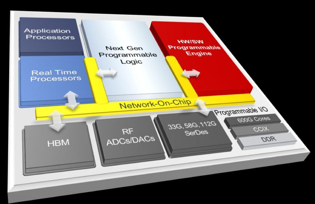
Figure 1: Block Diagram of Xilinx’s 7nm Everest architecture
All of the other major blocks in the above diagram appear in some form throughout the Xilinx 16nm Zynq, Virtex, and Kintex UltraScale+ families and need little elaboration. Those blocks include the Arm application and real-time processors, the programmable logic, HBM (high-bandwidth memory)—a stacked-die DRAM array attached to the Xilinx chip using a silicon interposer and 2.5D assembly techniques, RF ADCs and DACs, and high-speed SerDes ports.
But that big red box was a mystery. Intentionally so. It’s all part of the company’s dance of the seven veils that slowly reveals Everest/ACAP product details to maintain public interest while the device is still being designed. (Who would have guessed that noted writer and playwright Oscar Wilde would develop a marketing technique favored by high-tech marketers and reality TV celebs a century later?)
One or two of the veils hiding the mystery of the HW/SW Programmable Engine fluttered to the stage floor last week at the Hot Chips 30 conference held in Cupertino, California. That’s when Juanjo Noguera, engineering director of the Xilinx Architecture Group, gave a detailed presentation titled “HW/SW Programmable Engine: Domain Specific Architecture for Project Everest.” Noguera’s presentation provided many, many additional hardware details while keeping a few of the most interesting details veiled. Wilde would have been pleased.
The Everest HW/SW Programmable Engine is a tiled array of coarse-grained, software-programmable, VLIW vector processors connected to each other in multiple, hardware-programmable ways. According to Noguera, the VLIW vector processors can handle a variety of fixed- and floating-point data types. The HW/SW Programmable Engine tile array arrangement appears in the upper-left corner of Figure 2 below, while the individual tile detail with the interconnect scheme appears lower and to the right in the figure.
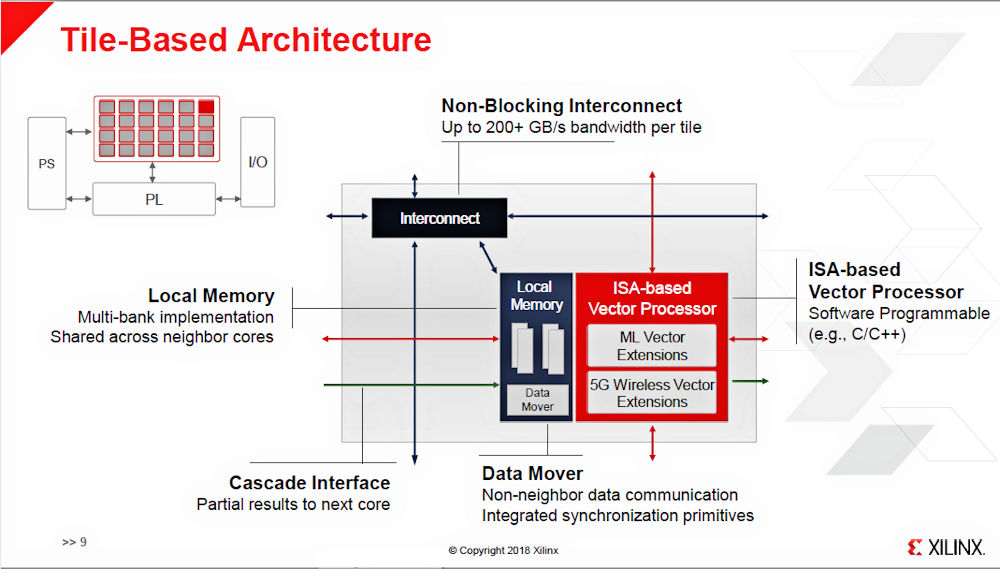
Figure 2: Detail of Xilinx’s tile-based HW/SW Programmable Engine for its Everest architecture
The HW/SW Programmable Engine array communicates independently with the PS (processor system) and the PL (programmable logic) in the Everest design. Each tile in the array consists of a software-programmable, VLIW vector processor coupled to local memory and a data mover (a DMA machine).
Three types of interconnect link tiles in the array. The first type, represented by the small red arrows in Figure 1, are parallel, bidirectional, word-level interfaces linking each tile to its four nearest neighbors using an NSEW (north, south, east, west) arrangement. In addition, the small green arrows shown in the diagram are unidirectional cascade interfaces that permit one tile to directly pass partial results to its adjacent, right-hand neighbor.
These short, local, point-to-point connections are reminiscent of the local interconnects used for short-range LUT-to-LUT communications incorporated into FPGA arrays, and the cascade interfaces resemble the carry bits between DSP slices. Certainly that’s not a coincidence, given that these sorts of communication paths have long been common in Xilinx devices.
For longer communications paths within the tile array, the HW/SW Programmable Engine uses a 200Gbytes/sec, non-blocking, deterministic NOC (network on chip). The NOC, plus the parallel local interconnect, constitute the “hardware-programmable” aspect of the HW/SW Programmable Engine.
You can connect the vector-processing tiles in a variety of ways to implement varied processing arrays. Noguera discussed five such configurations as examples in his talk. These examples appear in Figure 3 below.
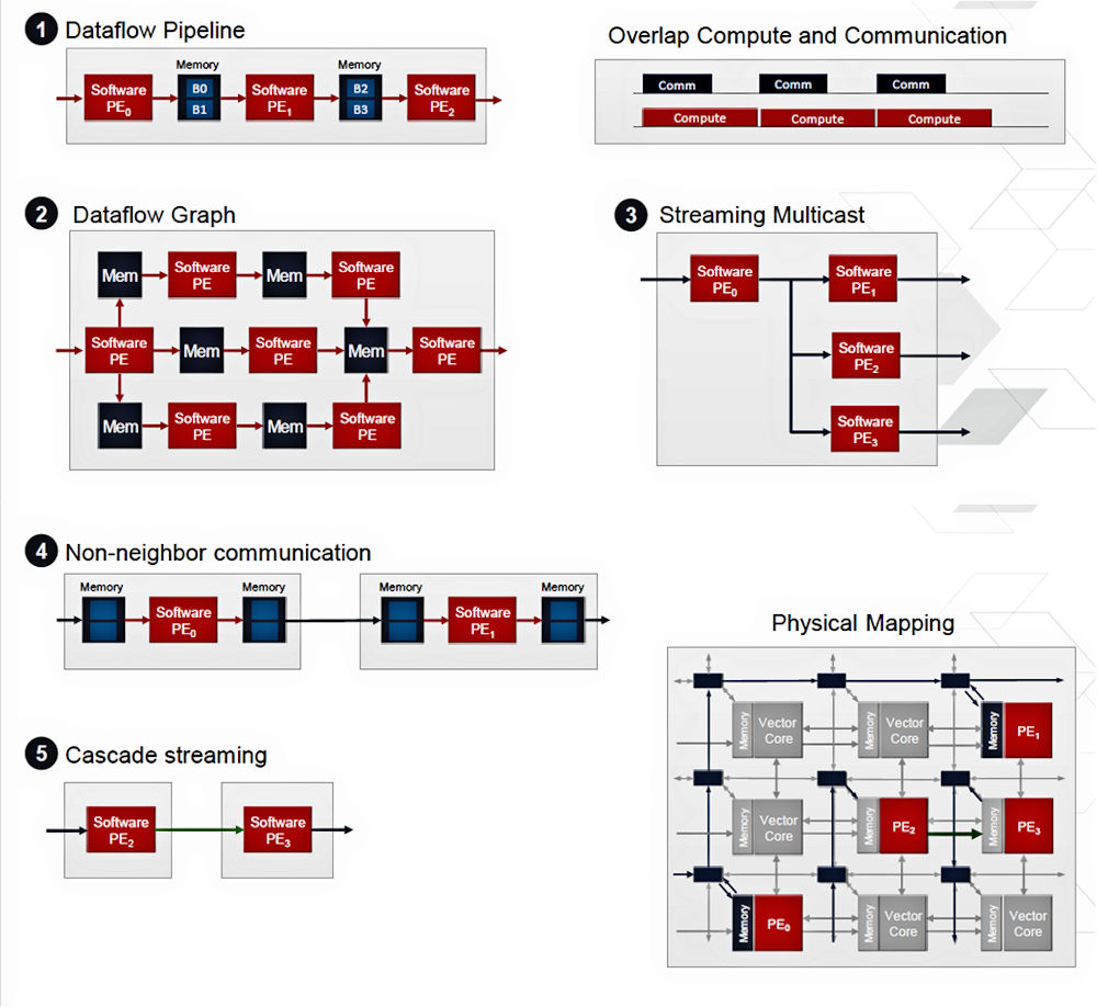
Figure 3: Sample processing configurations for the Everest HW/SW Programmable Engine.
Configuration 1 is a simple one-dimensional, unidirectional dataflow pipeline. Each processing tile partially processes an incoming stream of data and then passes the result through a local memory buffer to the next tile in the pipeline. Configuration 2 implements a dataflow graph, which might be considered a 2D, 3D, or more-D version of a pipeline. Essentially, it’s still a pipeline but with pipes running in multiple dimensions. Configuration 3 takes advantage of the NOC to multicast results from one processing tile to two or more subsequent tiles simultaneously. Configuration 4 uses input and output memory buffers to match variable, differential processing rates for tiles connected over the NOC. Configuration 5 uses the tiles’ cascade interface to pass intermediate results from one tile to the next without consuming other interconnection resources.
These are only five configuration examples. There are certainly more processing configurations to be invented using this new processing resource and, just as certainly, there’s room for some clever automation that can synthesize and optimize configurations to meet high-level performance and power goals. Of course, these interconnect schemes can be used in combination as well.
The HW/SW Programmable Engine’s capabilities can be extended using Everest’s on-chip PL, which is attached to the HW/SW Programmable Engine’s NOC through multiple NOC nodes and CDC (clock-domain-crossing) buffers, as shown in Figure 4. (Clearly, the architecture needs CDC buffers because the HW/SW Programmable Engine runs at a different clock rate than the PL. I’m guessing it doesn’t run slower.)
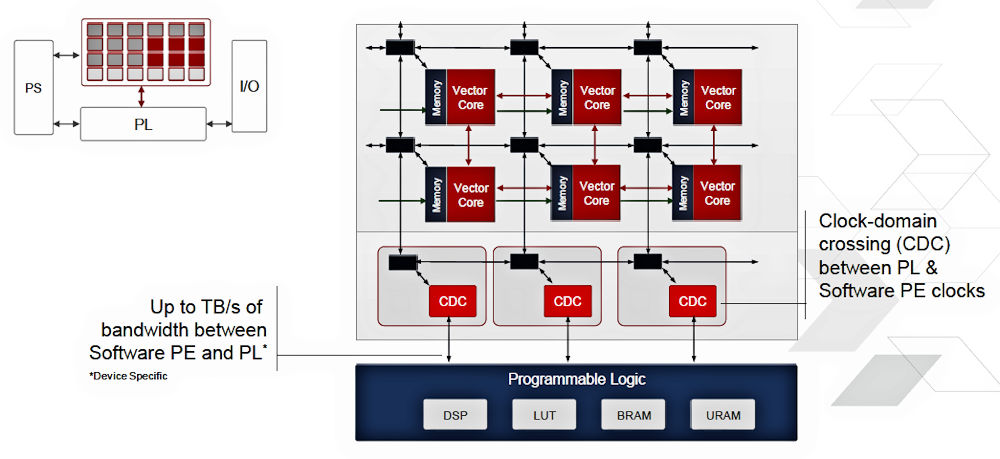
Figure 4: The HW/SW Programmable Engine’s NOC connects to the device’s programmable logic through multiple NOC nodes and clock-domain-crossing buffers.
As the figure states, the aggregate interconnect bandwidth between Everest’s HW/SW Programmable Engine (abbreviated “PE” in the figure) and its PL is on the order of Tbytes/sec. That figure that will cause many system architects to rethink their assumptions about processing architectures.
You can use the connected PL to augment the HW/SW Programmable Engine’s capabilities in multiple ways. For example, you can use the PL’s RAM arrays to increase the vector processing tiles’ access to on-chip SRAM (BRAM and UltraRAM) blocks in the PL with low latency through the deterministic NOC. It’s also possible to use the PL to implement hardware accelerators that can perform specialized computations faster than the tiles’ vector engines. Noguera suggested that you can also use the PL to create “ISA extensions” for the tiles, but he did not elaborate.
The performance results for machine-language inference and 5G wireless signal processing are impressive, as shown in Figure 5 below.
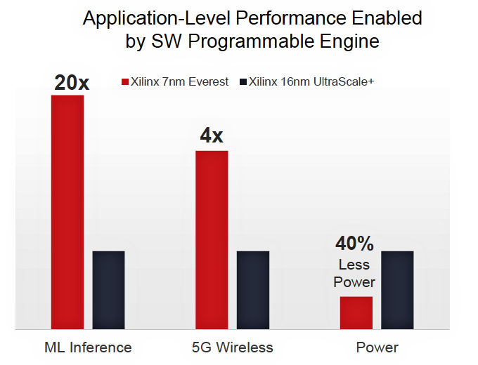
Figure 5: HW/SW Programmable Engine results relative to programmable-logic implementations.
The 20x improvement in ML (machine-language) inference is particularly noteworthy for its magnitude. FPGAs are already pretty quick when it comes to ML inferencing because the inference calculations involve many, many multiplications and additions. The thousands of DSP slices in an FPGA can perform those calculations quickly, but the HW/SW Programmable Engine appears to be even faster. The 4x improvement in 5G wireless processing is also significant, said Noguera, because it means that the Everest architecture can directly handle a transmission bit -rate of 2Gsamples/sec.
That statement led to some detailed questions from the audience during the Q&A following Noguera’s presentation. The first question was about the clock rate for the HW/SW Programmable Engine. Noguera answered by saying that he could not yet answer that question directly but that he was trying to provide indirect guidance by stating that the engine could handle a 5G transmission bit rate of 2Gsamples/sec. Operating frequencies for the HW/SW Programmable Engine’s processors would be “on the order of Giga,” he stated.
Another question dealt with the number of tiles in the HW/SW Programmable Engine’s array. The answer is that there will be tens to hundreds of tiles in each HW/SW Programmable Engine, depending on the device family member. ACAP devices with hundreds of vector processors in their HW/SW Programmable Engine will be massively parallel. This range is very consistent with the way all FPGA vendors, including Xilinx, place varying quantities of resources into individual members in broad device families, and it telegraphs Xilinx’s intent to develop a family of ACAP devices.
However, the first Everest device has yet to tape out. That milestone is scheduled to happen later this year. Meanwhile, the dance of the seven veils continues. Noguera promised more details would be disclosed at the Xilinx Developers Forums being held later this year in San Jose, Beijing, and Frankfurt. You might consider registering.


One thought on “Xilinx Puts a Feather in its ACAP”