


“Who’s on first, What’s on second, I Don’t Know is on third.”—Abbot and Costello
Recent news regarding progress made by semiconductor process technology’s major players has left me feeling like I’m listening to the classic Abbot and Costello “Who’s on First?” baseball comedy skit. Abbot and Costello are simultaneously hilarious and confusing in their rapid-fire delivery, and the situation is much the same with the self-proclaimed “true leaders” in IC process technology. Case in point: three recent earnings calls from Intel, TSMC, and AMD (Who, What, and I Don’t Know).
Who’s on First? Intel
Let’s start with Intel. During the company’s April 26 earnings call, Intel CEO Brian Krzanich said:
“We continue to make progress on our 10nm process. We are shipping in low volume and yields are improving, though the rate of improvement is slower than we anticipated. As a result, volume production is moving from the second half of 2018 into 2019. We understand the yield issues and have defined improvements for them, but they will take time to implement and qualify.”
Krzanich then said:
“…14nm process optimizations and architectural improvements have resulted in performance gains of more than 70% since the first 14nm products were launched. We combine these advances in manufacturing technology and architecture to produce true leadership products. And it’s that product leadership that ultimately matters most to our customers and end users.”
Translation: Volume production for microprocessors based on Intel’s 10nm process technology are yet again delayed, this time until 2019, but Intel claims technology leadership because its 14nm products are kicking butt.
What’s on Second? TSMC
TSMC conducted an earlier call that also contained significant technology news. On April 19, TSMC’s Co-CEO, President, and Additional Director C.C. Wei said:
“TSMC’s 7nm technology, in terms of performance, power and area density, as well as its schedule, is leading the industry. So far, we have already fabbed out more than 18 customer products with good yield and performance. More than 50 product tape-outs have been planned by end of this year from applications across mobile, server CPU, network processor, gaming, GPU, PGA, cryptocurrency, automotive and AI. Our 7nm is already in volume production.”
Later in the call, Wei said:
“Now I’ll talk about the N7+ and EUV. We believe we can extend the success of our 7nm to its enhanced version N7+, which will have 20% better density and greater than 10% power reduction. And N7+ will use a few EUV layers to replace the immersion lithography process. As a result, fewer masking layers can be used. As the N7+ will use more than 90% of the same tools with the N7 and N10, where we have fine-tuned all the advanced equipment to their optimum condition during their ramp-up, we believe we can leverage our production learning to N7+ and enjoy the industry’s best defect density among competitors of comparable technologies.”
“Our N7+ silicon results to-date are very encouraging. Not only have we demonstrated equivalent or better performance in yield on both 256Mbit SRAM and on a product-like test vehicle when compared to N7 baseline, we have also demonstrated a tighter distribution of electrical parameters in the layers where EUV is supplied. Since we maximize design rule compatibility between N7 and N7+, our customer can minimize the IP porting effect—effort—I’m sorry. A few customers have already planned to tape out the N7+ in second half this year and more in the first half next year. Our N7+ volume production is planned in 2019, which remains unchanged.”
Translation: TSMC’s first-generation 7nm N7 process technology is now in volume production and the company’s EUV-enhanced, next-generation N7+ process technology should be in volume production at about the same time that Intel expects its first-generation 10nm process technology to hit volume production.
I Don’t Know’s on Third. AMD [and Globalfoundries]
And then there’s the April 25 quarterly earnings call by AMD. During the Q&A following the scripted presentation, Timothy Arcuri of UBS Securities asked:
“I think you said that the 7nm [GPU] product is in the lab, and it’s going to launch later this year. That’s the product at TSMC, correct? And I guess, I’m just wondering – on that front do you feel comfortable that you can get capacity from that vendor?”
AMD’s CEO Lisa Su responded:
“So our foundry strategy is to use both TSMC and GLOBALFOUNDRIES on the first 7nm product. We are using TSMC for that product and we have a very strong relationship with them. And so, we do see a good momentum on it from what we see, and I’m not concerned about capacity.”
Now Su’s statement that AMD is using TSMC instead of Globalfoundries for its bleeding-edge GPUs is both news and not news. It’s news because Globalfoundries absorbed AMD’s fabs and process technology back in 2009 as part of its creation and therefore has a most-favored vendor status with AMD. If AMD chooses not to use Globalfoundries for its parts, there’s presumably a contractual fee due to Globalfoundries. It’s not news because AMD has been using TSMC and other vendors as alternate sources for some sub-28nm CPU and GPU products for a while now, so the GPU news isn’t all that extraordinary.
With both Intel and TSMC claiming process technology leadership, AMD’s call lends credence to TSMC’s claim, which now prompts the questions:
Who is leading the semiconductor pack, why does this matter, and who cares?
The Recap
Intel’s multiple delays on announcing 10nm volume production means that the 2019 prediction is the latest best estimate (also known as a guess) while TSMC’s announcement of 7nm volume production during an earnings call is a fact. At least it had better be a fact if it’s stated in an earnings call.
According to IC Insights’ McLean report, TSMC’s IC foundry income was $32 billion in 2017 while Intel’s income for foundry services was less than $1 billion (see Figure 1 below and note that Intel as a foundry doesn’t make IC Insight’s top-8 list).
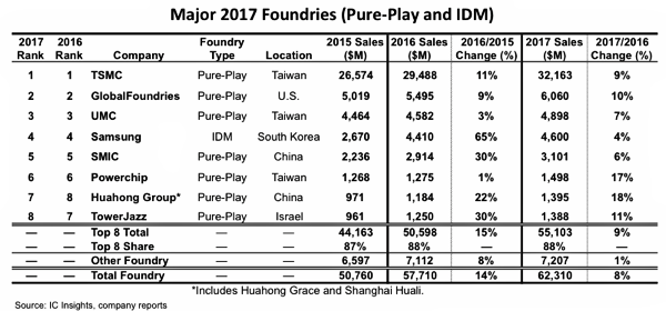
Figure 1: IC foundry ranking for 2017. Source: IC Insights
This doesn’t mean Intel isn’t a leader; It means Intel’s claimed industry leadership in process technology is mostly important to Intel and primarily for making Intel’s server and PC processors. It’s also somewhat important in other semiconductor markets where ICs fabricated from Intel’s and TSMC’s process technologies clash—namely in the FPGA realm.
Why’s in Left Field
Does Intel care if TSMC has process leadership? I doubt it. TSMC is helping Intel where it counts: revenue leadership.
On April 11, Intel announced that both Dell EMC and Fujitsu were the latest data-center server vendors to incorporate Intel Xeon Scalable Processors and Intel Programmable Acceleration Cards based on Intel Arria 10 FPGAs and the Intel Acceleration Stack. (See “Accelerating Mainstream Servers with FPGAs: Intel Puts FPGAs Inside” by Kevin Morris.)
Dell EMC introduced the PowerEdge R940xa and PowerEdge R840 data center servers based on Intel’s Xeon processors and its mid-range Arria 10 GX FPGAs at Dell Technologies World 2018 on May 1. Fujitsu is adding accelerator cards based on Arria 10 FPGAs to its PRIMERGY server line.
Those Arria 10 FPGAs are built on TSMC’s (NOT Intel’s) 20nm planar process technology. (See “Mid-Range Mayhem: The Best Blue-Collar FPGAs” by Kevin Morris.) Dell EMC and Fujitsu don’t seem to care that the process technology used to make these mid-range FPGAs isn’t the latest and greatest. Heck, they don’t even seem care that the Arria 10 FPGA silicon comes from TSMC.
Contrast these announcements with Huawei’s debut of its FPGA Accelerated Cloud Server (FACS) platform at SC17 last November and the fact that Amazon made its FPGA-accelerated EC2 F1 cloud service generally available more than a year ago. The FPGAs used in the Huawei and Amazon accelerated cloud servers are Xilinx’s most-current, top-of-the-line Virtex UltraScale+ FPGAs built with TSMC’s 16nm FinFET process. Perhaps it was the process technology that made the difference in the FPGA selection. Perhaps it was something else.
The Shortstop is “I Don’t Care”: Perhaps process technology isn’t the driver it once was.
Maybe process technology leadership matters, but it depends on what you’re doing and which Baseball Fantasy League you’re affiliated with. Are you developing your own ASIC? Then you’re likely talking to TSMC because they’re the largest IC foundry by a factor of five over the nearest competitor and they are happy to work with designs created with the leading IC EDA vendors’ design tools. In addition, TSMC is clearly one of the two IC process technology leaders if not THE technology leader. (Depends on who you ask, doesn’t it?)
Are you buying packaged server or PC processors? Then you’re likely talking to Intel unless you’re a dyed-in-the wool maverick, a charter member of the “Anyone but Intel” league, or a patron of the “cheap and cheerful chips” baseball club.
If you’re buying packaged FPGAs for system designs, then you’re more likely to be looking at many device specs other than process technology, including the amount of on-chip logic, DSP blocks, and memory; the number and data rates of the on-chip, high-speed SerDes transceivers; or some other critical functional characteristics that actually contribute to meeting system design goals. Process technology is one degree removed from these specs.
For system designers, it’s the functional specs, the design tools, and the support that wins the ballgame.


