


You’ve driven it for a decade or more. It’s taken you on-road and off-road. It’s brought you to the corner store and across the country. It’s got over 200,000 miles on it, and it’s still running fine. The thing is, you know you’re going to need to upgrade one of these days. Will the car die and force you into a decision? Or will you be able to plan ahead for a managed transition?
After all, you haven’t had a car payment in years, and new cars, well, they have all these crazy high-tech features – and yet, if you can hold out just a few more years, they may be even higher-tech. So… maybe fix the brakes and put some new tires on it? Or is that putting good money into a failing proposition? If only there were one thing that could hold you over a bit longer, that could ensure that you’ll get more life out of the old beast…
For all the flash and splash of spiffy new technologies, sometimes it’s fine just hanging out, watching the young bucks slay each other in the streets with here-today-gone-tomorrow ideas while you sit back on the porch enjoying that mint julep… Moving from one silicon process node to the next one can be disruptive, so, if you can string it along a bit longer, why not just stick around? Why rush things?
At each node, some challenge from the prior node gets addressed. Sometimes that has meant a massive change – say, high-Κ metal gates or FinFETs. Others perhaps are not so dramatic. Well, a company called Atomera has modified the basic transistor in a way that improves carrier mobility and reduces leakage – tweaks intended to let you postpone that move to the next node.
2D Currents
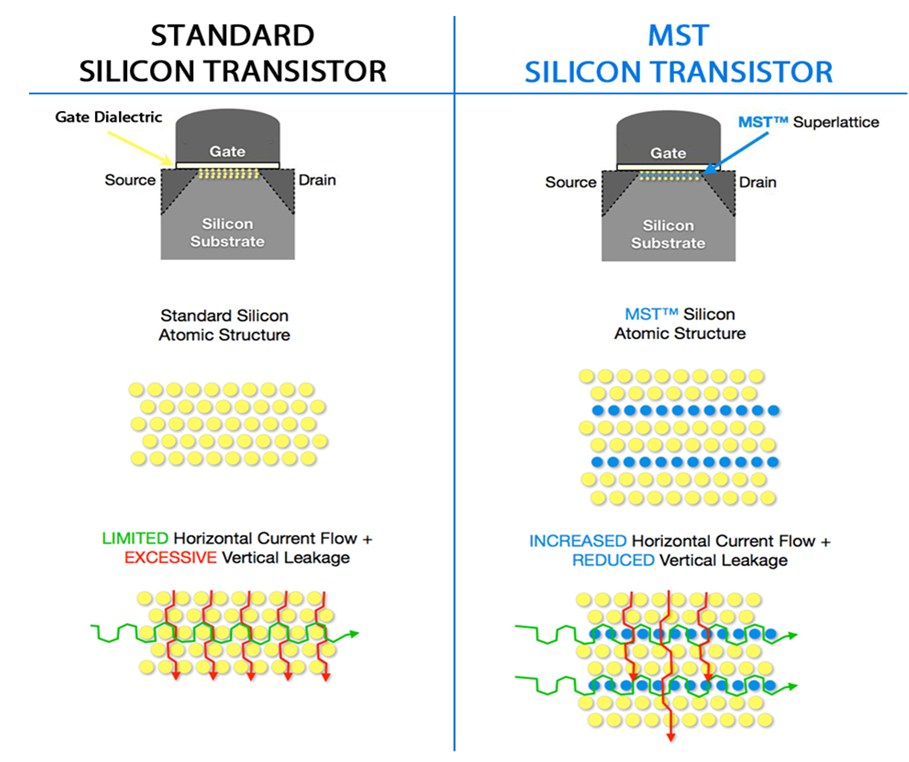
At this point, we’re still talking good old-fashioned planar transistors – let’s pick the 130-nm node as an example. Atomera paints a picture of currents in two directions. In the horizontal plane, you have the current that’s doing work for you. The more easily it flows, the faster your work gets done.
Meanwhile, in the vertical direction, you have leakage current drifting down into the bulk. You’ve lived with it, but you’d prefer to live without it.
Well, picture a four-lane highway – two lanes in each direction. One slab of asphalt with painted lines showing where you’re supposed to be. That can work fine for a while, until traffic gets too heavy. Then drivers are going to become impatient, changing lanes rapidly and unpredictably – even drifting into oncoming traffic in order to gain some positional advantage.
Under those conditions, drivers are going to slow down a little, since you never know which of the cars around you contains the goofball that will put everyone’s lives at risk for the sake of 20 feet of pavement. So what do you do to make things better?
Jersey barriers, of course! A nice long line of concrete separating the two directions of traffic. Heck, if things remain squirrely after that, you can even put barriers between the lanes going the same direction, with breaks for exits and entrances.
Freed of the constant risk of kamikaze craziness, drivers can relax a little – and speed up. Everyone will be going straight. Improved forward mobility; no cross-traffic.
Which is the essence of what Atomera calls Mears Silicon Technology, or MST (after founder Robert Mears). As illustrated below, they build layers of oxygen that act as the Jersey barriers, confining current to the horizontal direction.
(Image courtesy Atomera)
These aren’t deposited thin-film layers; they’re grown epitaxially, ensuring that the oxygen atoms are firmly bound into the crystal structure in a manner similar to the way strain is added. Apparently, absent that firm bonding, the oxygen would have a tendency to wander away like an unsupervised puppy.
The minimum layer thickness is in the 10s of angstroms, although they typically lay down a couple hundred angstroms’ worth. It happens between the well implant and the gate.
The Jersey barrier analogy breaks down a little bit if you look closely at the right side of the figure above. The “traffic” isn’t confined between the added barriers; that traffic in fact now uses those barriers as a preferred path. Hence higher mobility. Meanwhile, the vertical leakage is blocked.
In addition to providing this current confinement, it can also help engineers to tailor doping profiles, essentially providing dopant confinement.
While we’ve set this up as a stay-on-the-current-node thing, the benefits they tout are more nuanced. After all, if your transistor currents go up more than you need, you may be able to downsize and save space. They listed three specific examples of accrued benefits in three different applications:
- Smartphone battery life extended by around 50%
- A power-management IC (PMIC) with reduced power consumption and a 15-20% die-size savings
- They even talk about enabling a new class of mobile double data-rate memory.
And the cost? They claim that it’s nominal – disappearing into the cost of the smartphone example and actually enabling a cost reduction on the PMIC. They say that they’re being reasonable with royalties, presumably in the hopes of encouraging this as the future default way transistors are built.
In theory, it can also work on 3/5 materials and with FinFETs, but, other than some simulations, they haven’t focused their energy there. They see particular value in helping customers postpone two of the more difficult node transitions: 130 à 90 and 45 à 28.
And the status as of this moment? Well, believe it or not, these guys have already IPOed – and we’re still some distance from commercial usage. They are now in Synopsys’s TCAD tools, so foundries and fabs can optimize them and work them into their PDKs. Circuit designers will eventually interact with them via those PDKs. They won’t be involved in any of the detail; it will simply be another transistor choice.
Evals are underway now, putting commercial availability into the 2019 timeframe – assuming the evals finish cleanly without the need for any further data.
So yeah, buff up the old beast a little bit; put some air in the tires; give it a fresh draught of oil. You may find you have lots of miles left.
More info:


What do you think of Atomera’s approach to improving transistor carrier mobility and reducing leakage?