


For years we’ve had two possible levels of integration. Most electronic functionality was assembled at the board level, with components soldered down. If you really had some volume in mind, you could integrate the functionality onto a single chip – and the more we move into the future, the more we can integrate.
More recently, we’ve found a middle way: 2.5 D and 3D integration. 3D means stacking chips and wiring them together, either with bonding wire or with microbumps connected to through-silicon vias. 2.5D, on the other hand, involves chips placed onto an interposer.
An interposer is like a little mini-PCB, except that, in the case of a silicon version, it’s made out of crystalline (or even polycrystalline) silicon instead of some organic material like FR-4. That means much more aggressive rules on line widths and spacing, so you can pack dice far more densely than would be possible on a PCB. The rules are also much more consistent; none of this, “Yeah, that violates the rules, but, in this case, we think it will be OK; go for it” stuff.
But here’s a challenge with all three of those scenarios – PCB, IC, 2.5D packaging. All three must be explicitly designed, and, once assembled, they can’t be changed. They also take time to realize – and for today’s designers charging into evanescent markets like those presented by the Internet of Things, getting something out as soon as possible is critical. That, of course, is one of the motivations behind programmable logic – having some freedom to modify functionality even after everything else has been locked down. But connectivity mostly hasn’t been the major motivator of that solution.
Unless, of course, you have a long memory. Anyone remember Aptix? They made… well, the word “interposer” wasn’t fashionable back then, but they built what was essentially a connectivity substrate on which you could place chips and then program the way they’re connected.
I’m not really sure how good (or not) the technology was, but it more or less didn’t matter – since things got completely overshadowed by non-technical issues of an astonishing nature. So Aptix is no more, and there were no further visible attempts at something similar.
Until now. A company called zGlue has announced a new such substrate (in principle), built with different technology and with some updates to how the connections are managed. We’ll look through it here, and you can decide whether it has a better future (barring any drama).
Be Seated, My Little Chiplet!
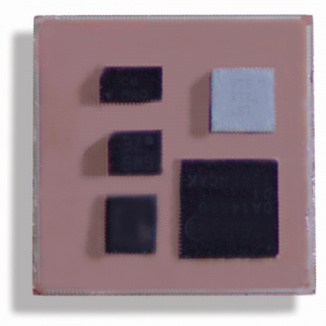
Before we dig into the zGlue substrate, we need to come to grips with a new term – ok, it was new to me, anyway. Imagine taking a full-on chip, like a microprocessor, and disassembling it into basic blocks: the CPU, the cache, the memory-management unit – you get the picture. Each cast separately into silicon. And now you reassemble the whole thing by connecting those pieces back up – maybe in a way that differs from the original.
Each of those pieces, which amount to the hardest possible IP, is a “chiplet.” This is a clue to the level of assembly we’re talking about. We’re not assembling packaged parts with pins; we’re not even assembling entire dice at the chip scale (although you could). No, we’re assembling little silicon IP blocks.
The chiplet notion appears to date back to 2013, when Xerox PARC issued a new vision involving miniscule chiplets that could be assembled even by turning them into ink. That latter part of the vision is not part of the zGlue solution, but they’ve adopted the chiplet notion as silicon embodiments of IP blocks.
This raises the obvious question, “Where would I obtain said chiplets?” And, if you’re a modern practitioner of technology, you respond with the obvious answer: “From a chiplet store, duh!” Which would, of course, be online. This is what zGlue is building as part of their support ecosystem; they call it the ZiPlet Store.
An Active Substrate
If we look at the old Aptix technology, it consisted of antifuses that would be blown where a connection was desired. That’s it. For sensitive signals, the resistance and capacitance of those connections would require inclusion in any electrical analysis, as signal quality might be affected.
The zGlue approach appears to be quite different. Rather than thinking of this as an interposer or strictly as a connection matrix, it’s better to think of it as a full-on chip that happens to have lots of landing sites on the top for the chiplets. So, for example, the signals are actively managed, although I don’t have details as to how that’s done. There are even built-in passives that can be connected per the requirements of any chiplet.
And, if that’s not enough, there’s also a built-in power management block. So we have a fair bit of analog circuitry acting in a support role.
In yet another departure from Aptix, the connections will not survive a power down. They must be re-established at power-up; they say that the configuration time is in the range of micro- to milliseconds.
The design idea, then, for users of this technology, is that, using a tool called zCAD, you take the chiplets you obtained from the store and you drag-and-drop them into place. The tool then automatically routes the connections.
 (Image courtesy zGlue)
The flexibility afforded by a solution like this can be of obvious value when prototyping: you can change connections dynamically as you refine the design. But the next question always comes down to cost when entering commercial volume production. Are you going to use this to get to market quickly and then completely redo the design using simple interposers to reduce costs?
This takes me back many years to the first programmable logic device that saw volume success: the PAL (for Programmable Array Logic). The same discussion occurred then: how do you reduce the cost of a programmable solution once the programmability is no longer needed? At the time, the response was the HAL – for Hard Array Logic. And there were two possible ways to do this.
Bipolar transistors were the order of the day, and TiW fuses were how connections were made (it was a subtractive technology, where unneeded connections were eliminated). So one solution to hardening was to leave out the fuses entirely and replace the intended intact fuses with metal lines.
“But,” you say, “that doesn’t save any die area.” You’re right. But it does mean that you no longer have to test the programming circuitry, since it’s not needed. Yields go up, reducing cost. For even higher volumes, a dedicated hardened die could be designed – one that eliminated the programming circuits altogether for yet more cost savings.
In the zGlue case, you have two production models. For moderate volume, you include the configuration pattern in the firmware, loading at power-up. For very high volumes, they have a hardening strategy – although I couldn’t get much specificity on how that works and where the savings come from.
They also claim a number of security features, although, again, I’m light on details. They have implemented some anti-tampering features – for instance, if you remove one of the chiplets, the substrate will know. The design connection information is hidden and can be encrypted if desired. And they’ve implemented some key management, using OTP memory to store keys.
Not in the Store
This sounds ok so far, but there’s an obvious question. If you’re simply in the business of assembling existing blocks, then presumably you’re adding value by doing so in a way that’s novel and unique. But most circuits involve islands of secret sauce. (I know, sounds like an Arthur Conan Doyle title: The Mysterious Islands of Secret Sauce). Much of the product differentiation will arise from that secret sauce.
So you can get lots of the surrounding circuitry from the store, but what about stuff that’s not there? And, in particular, your own stuff – which you’d never put in the store?
There are a number of options for handling this. If the missing chiplet is more or less generic – that is, it doesn’t constitute secret sauce – then you can add it (or ask that it be added, depending on the IP owner) to the ZiPlet Store.
The thing is, that will make the new addition available to anyone else buying from the ZiPlet Store. You don’t want that happening with your secret sauce; you want exclusivity. If you own the chiplet in question, then they say that you can connect it via zCAD. If the chiplet is owned by a third party, then some negotiation might be required to make it available on an exclusive basis – which may include some added cost.
The integration and any analysis of power or timing will, of course, need to take the zGlue chip characteristics into account. They license the technology to foundries, so the details may, in principle, vary depending on which foundry is used. A separate OSAT subcontractor will handle assembling the chiplets on the zGlue substrate; that completed unit can then be shipped to the company tasked with assembling the final circuit board. Or, if the contents of the zGlue substrate make up the entire circuit, then it becomes your PCB; you don’t need to put yet another PCB under it.
Will this see better traction than the old Aptix technology? That’s not a fair question, given the extraordinary events back then. zGlue does appear to have been more aggressive about including enough support circuitry to ensure good performance. We’ll have to wait to see if it truly catches on, however.
More info:


What do you think of zGlue’s programmable “interposer” substrate?