


“Don’t look back. Something might be gaining on you.” – Satchell Page
Dave Jones, the multitalented proprietor of EEVblog.com has posted more than 1100 online videos covering all aspects of electronics, including numerous teardown videos that I used frequently in a prior life to highlight certain revealed design aspects in the equipment he’s torn down. Recently, Jones posted a 1-hour (!) teardown video of the new Siglent SVA1015X, which is a low-cost, combo spectrum analyzer (SA) and vector network analyzer (VNA). The Siglent SVA1015X SA/VNA sells for $1395, configured as an SA. Add $609 to that price and you get the VNA option. There’s another $2K or so of software-enabled options available beyond that.
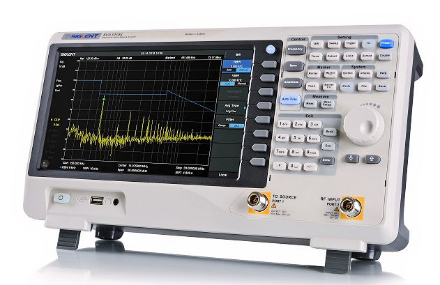
Figure 1: Siglent recently introduced the low-cost SVA1015X spectrum analyzer/vector network analyzer. (Image Source: Siglent America)
The SVA1015X hides a lot of RF engineering under its hood. But, as a processor sort of guy, I’m going to focus on the digital design of this instrument because it reveals the evolution in Siglent’s design approach when compared to the design of the SSA3021X spectrum analyzer that Siglent introduced back in 2016. Conveniently, Jones tore down that earlier instrument as well. So that’s where we start.
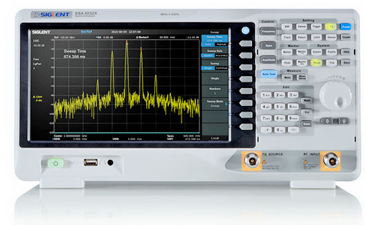
Figure 2: Siglent introduced the SSA3021X spectrum analyzer in 2016. Its external appearance is remarkably similar to the just-announced SVA1015X SA/VNA, but the internals are somewhat different. (Image Source: Siglent America)
The digital design of Siglent’s SSA3021X spectrum analyzer is consistent with many similar Siglent instruments in that it pairs an application processor—a TI AM3352 Sitara processor in this case—with an FPGA—a Xilinx Spartan-6 LX45. The TI AM3352 Sitara processor incorporates an Arm Cortex-A8 application processor, a 64Kbyte level-1 cache and a 256Kbyte level-2 cache, a DRAM controller, an LCD controller, and an assortment of other useful peripherals. Although the device’s Arm Cortex-A8 processor includes Arm’s NEON SIMD coprocessor, you wouldn’t really consider it a high-performance DSP.
Spectrum analyzers require a fair amount of signal processing, and that’s no doubt why the design of Siglent’s SSA3021X spectrum analyzer includes the Xilinx Spartan-6 LX45 FPGA—with its 58 on-chip DSP blocks—that gives you 58 high-speed MACs (multiplier/accumulators) to throw at whatever signal processing you need to perform. That’s far more MAC power than you get in your typical DSP.
Because both the Sitara processor and the Spartan-6 FPGA are packaged in BGAs, the Siglent SSA3021X SA’s large main board must be a multilayer pcb to connect the hundreds of signal traces to the solder balls on these BGA packages and to provide adequate power supply decoupling. Based on its “ZCZ” part-number suffix, the TI Sitara processor is packaged in a 324-pin BGA with the balls on 0.8mm spacing and the Spartan-6 LX45 FPGA is packaged in a 676-ball BGA with 1mm ball spacing. In total, that’s exactly 1000 pins split between the two devices.
Based on visual inspection, the spacing of the solder balls and the number of balls on these devices require more precisely-controlled pcb fabrication, smaller traces, and smaller trace spacing than is needed for the rest of the components on the Siglent SSA3021X spectrum analyzer’s main board. But there’s only the one large main board in this design, so the presence of these two BGA packages increases the manufacturing cost of the lone bare pcb.
Figure 3 shows a cropped close-up photo of the Siglent SSA3021X spectrum analyzer’s Sitara processor and Spartan-6 FPGA on the SSA3021X’s main pcb, as taken by Dave Jones:
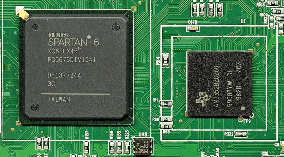
Figure 3: The TI Sitara application processor (on the right) and the Xilinx Spartan-6 FPGA in the Siglent SSA3012X spectrum analyzer are packaged in BGAs, which will increase the main pcb’s fabrication cost. (Image Source: Dave Jones/EEVblog.com)
A fair amount of engineering goes into a board like this. For example, look at the meandering (zig-zagged) pcb traces. These meanders temporally align the signal timing between the Sitara processor and the Spartan-6 FPGA by adding trace length to increase the signal delay in some of the traces. You can also see at least four differential matched signal pairs snaking away from the Spartan-6 FPGA at the lower-left corner of the photo. Two of the differential-pair traces also meander. Creating and verifying these precisely drawn pcb traces takes extra time, effort, and care, which adds development cost.
If you now look at the digital processing section of the new Siglent SVA1015X SA/VNA, as shown in Figure 4, you’ll see that Siglent’s spectrum analyzer design philosophy has changed significantly in the past two years, at least for the digital portion of the instrument. Instead of pairing an application processor chip with a separate FPGA as with the SSA3021X, Siglent has used a Xilinx Zynq SoC for the SVA1015X.
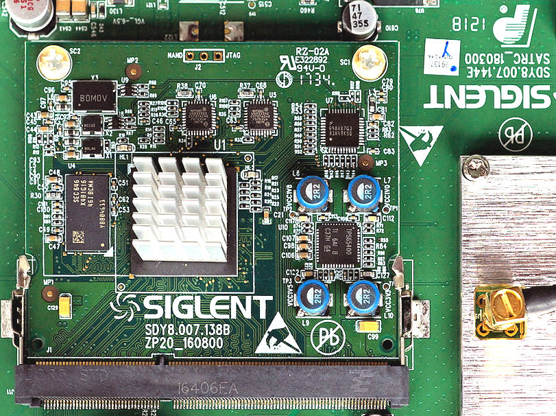
Figure 4: Siglent’s SVA1015X SA/VNA is designed around a processor daughter card that employs a Xilinx Zynq SoC (beneath the heat sink) instead of a separate application processor and FPGA. (Image Source: Dave Jones/EEVblog.com)
The Zynq SoC combines the application processor, memory controller, and peripherals with an FPGA—all on one chip.
Note: We know it’s a Zynq SoC because Jones connected a serial port sniffer to the Siglent SVA1015X’s UART debug port on the main board, which spit out the boot sequence listing shown at 16:50 in Jones’s video. The listing clearly shows there’s a Zynq SoC booting a Linux kernel in the Siglent SVA1015X SA/VNA; however, it doesn’t specify which Zynq device, and Jones didn’t peel off the heat sink to reveal the device number as he often does.
The layout of this board is significantly simpler than the board shown in Figure 3 above, but look carefully and you’ll see that the Zynq SoC isn’t soldered to the main board at all. Instead, the Zynq SoC and a companion SDRAM memory chip reside on a relatively small daughter card equipped with an edge connector that plugs into the instrument’s main pcb.
I counted the connector pins at the bottom of the photo in Figure 4, and it appears that Siglent has employed a standard, 204-pin DDR3 SODIMM socket for its daughter card (obviously sourced from TE Connectivity, based on the logo stamped on the right side of the connectors in Figure 4 above). Repurposing an existing, well-proven, high-volume connector technology in this manner represents very cost-effective engineering design.
Siglent’s approach to digital processing inside of its SVA1015X SA/VNA confers at least three significant design benefits. First, it greatly increases the connectivity between the dual-core Arm Cortex-A9 application processor and the FPGA within the Zynq SoC. Referring back to Figure 3 and the design of the main board for the SAA3021X SA, you can easily count the number of visible connections between the Sitara application processor and the Spartan-6 FPGA. You can also get a sense of the design effort needed to make these connections by again looking at all the timing-compensation meanders in many of these interconnecting traces.
The Zynq SoC has the equivalent of more than 3000 pcb connections running between its dual-core Arm Cortex-A9 processor and the on-chip FPGA fabric. That’s far more connectivity and therefore more bandwidth than is possible with a 2-chip processor/FPGA design (most BGA packages just don’t have that many pins) and the connections are already predesigned, debugged, and fabricated for you.
Second, having the processor-to-FPGA connections on chip and mounting that chip with its SDRAM on a daughter card reduces the fabrication cost of the instrument’s main board because that large pcb no longer needs to accommodate fine-pitch BGAs, which should eliminate at least a couple of inner layers on the main board.
Third, it gives Siglent engineers more flexibility in selecting the digital processing chip. Low-end Zynq SoCs comprise a family of very similar devices that offer increasing amounts of FPGA along with identical dual-core Arm Cortex-A9 application processors. Should Siglent require more processing power—signal-processing power—then it can step up the daughter card design from one low-end Zynq member to the next. The new daughter card would then plug into an unchanged main board. This design approach makes it much easier to develop mid-life performance kickers for the existing instrument or even entirely new products.
What kind of signal-processing power are we talking about? The Xilinx Spartan-6 LX45 FPGA has 58 on-chip DSP48A1 slices. You’ll find an 18×18-bit MAC at the core of each of the DSP48A1 slices. Signal-processing algorithms hunger for MACs. When it comes to DSP algorithms, the more MACs you have, the faster you go. That’s a major reason why FPGAs have displaced DSPs from most signal-processing applications. FPGAs have a lot more MACs.
The smallest Zynq SoC, the Z-7010, contains 80 DSP48E1 slices, and you’ll find a 25×18-bit MAC at the core of each of those DSP48E1 slices. That’s already more processing capability than Siglent gets from the Spartan-6 LX45 FPGA. Should Siglent decide to develop an upgraded instrument that needs additional DSP capability, the Zynq Z-7015 SoC contains 160 DSP48E1 slices and the Zynq Z-7020 SoC contains 220 DSP48E1 slices.
Meanwhile, the instrument’s RF analog-processing block and tracking-generator block are also modular, and they, too, can be upgraded without changing the main board. This is an excellent way to design product families that give your customers more reasons to buy from you.
But wait. Xilinx announced the Zynq SoC in 2010. It’s been shipping for quite a while, so the question then becomes: “What took Siglent so long to change?”
One clear answer is surely ever-present engineering inertia, which appears in at least two forms. One source of engineering inertia can be characterized as “existing code” or “existing design.” If you’ve developed proven, working software for an application processor or have a working design in an FPGA, you’re loath to chuck that work without a darn good reason. IP reuse is a great idea, and, “If it works, leave it alone,” is one of my iron-clad engineering mantras.
Another form of engineering inertia comes in the form of tool-chain affinity. Once you and your development team learn the quirks, foibles, and workarounds of a development tool chain, you’re not likely to jump at the chance to adopt a new one—at least not without some compelling reason. In making the undoubtedly painful jump from the Sitara/Spartan combo to the Zynq SoC, Siglent’s design team had to leave the TI software-development and Xilinx ISE FPGA-development tool chains behind and replace both with Xilinx’s Vivado. They may have managed to drag some existing code along with them, but there’s still a real learning curve involved here. It took determination to make the jump.
The most compelling reason to make such a change, in my experience, is competitive. If you’re not updating and advancing your products’ designs and if you’re not using the most advanced component technology available, then your competition’s likely catching up to or bypassing you. In electronics, if your products occupy a desirable niche, you can bet something’s gaining on you.
Even if you don’t know it.
But there’s another reason for the change that’s apparent from even the most cursory comparison between the SVA1015X and the SSA3021X. The SVA1015X can operate as a spectrum analyzer and, optionally, as a vector network analyzer. The SSA3021X is only a spectrum analyzer. Although the SSA3021X has a tracking generator option that permits swept-frequency analysis of RF response, that’s just not the same thing.
I’m going to make a small guess here and say that the Zynq SoC’s extra signal-processing power came in mighty handy when Siglent’s engineers designed the new vector network analyzer capability.
Why keep the SSA3021X in the Siglent product line if it uses older technology and lacks the vector network analysis capability? Thanks to its superior and more expensive RF modules, the SSA3021X has somewhat better input bandwidth (9KHz to 2.1GHz versus 9KHz to 1.5GHz) and a 5db lower noise floor compared to the SVA1015X, so why not keep it? Considering the close physical similarity between the SSA3021X and SVA1015X instrument packaging, it’s certainly possible for Siglent to adapt the SVA1015X’s new main board and daughter board designs to the SSA3021X’s RF modules to create a 3000-series VNA with more RF bandwidth.
Finally, this may seem like an all-Zynq article, but that’s because of Siglent’s choice of the Zynq SoC for the SVA1015X SA/VNA. However, you are not limited to the Zynq family or even to Xilinx if you decide that your design would also benefit from the use of a processor/FPGA combo device. Intel offers similar processor/FPGA chips that it calls SoC FPGAs—also based on a dual-core Arm Cortex-A9 application processor—in two of its three major FPGA product lines: Arria and Cyclone. Microsemi (now owned by Microchip) offers devices that it too calls SoC FPGAs in its SmartFusion and SmartFusion2 families. The SmartFusion and SmartFusion2 devices are based on the smaller, slower, single-core Arm Cortex-M3 processor. Intel’s and Micosemi’s SoC FPGAs offer similar design and performance advantages compared to the Zynq SoC, realized by closely coupling processors and FPGAs on the same piece of silicon.
And yes, there are higher-end parts on the market now from Intel and Xilinx: the Intel Stratix 10 SoC FPGAs and the Xilinx Virtex UltraScale+ MPSoC. Both of these product families are based on the latest silicon tech from their respective makers and employ multiple 64-bit Arm Cortex-A53 processors along with more advanced and larger FPGAs. Given that it’s taken eight years or so for the Zynq SoC to go from initial announcement to incorporation into Siglent’s low-cost SVA1015X SA/VNA, it may take a while for these newer Xilinx devices to start appearing in similar equipment, but the need for more and faster processing never seems to abate, so don’t count on it.


