


Anytime the new cool thing comes around, all the cool engineers have to figure out the best ways to make it work. And we embark on a natural progression – or perhaps succession is a better word – sort of the way a depression along a river changes from pond to wetland to meadow.
In this case, the succession all about the conflict between flexibility and cost. (And performance.) In general, you can get either performance or one or both of the other two. The thing is, though, that, if the best way to do the new thing isn’t known yet, then you’re likely to settle for something suboptimal for the sake of flexibility, figuring it out as you go, and perhaps fixing it after it’s deployed in the field.
In other words, in the early days, you’ll use software.
After that, you might move to hardware of the flexible sort: FPGAs. You can still figure things out and make changes, but you get better performance (and maybe better cost, unless your software version was dog-slow).
After this, you can transition to ASIC. But do you go there directly? Maybe not. Maybe you have an ASIC chip with selective flexible hardware. Or maybe you have flexible hardware with selective hardened blocks to improve cost and performance. Either way, there are steps between totally programmable hardware and completely hardened hardware.
The Latest New Kid in Town? AI
Everyone wants in on AI. It’s the latest thing that your board members want to make sure you can put on your prospectus – even if you’re making peanut butter. “What’s our AI story?” “Um… we optimize the mix of peanuts using machine-learned algorithms?” “Ah, OK, good. Customers will eat that up!!” “Um, yeah, OK.”
So, since everyone wants a piece of AI, then they’re going to need some way to do AI. Software’s been the thing, and, there, the succession has been CPUs to GPUs and, in some cases, thence to FPGAs. Of course, we’ve seen a variety of IP blocks incorporating DSP blocks and other processing units used for SoCs – especially when implementing vision applications. But that’s still software on a processing block tailored for vision AI. Still early in the succession.
At some point, we’re going to need actual ASICs. But are we yet to the point where we know the best way to implement AI? No, we’re not. And there probably isn’t really any such endpoint, since what works best is likely to vary by application.
So how do we keep moving along the succession?
A Neu Approach
eSilicon has announced their neuASIC neural-network platform. And it’s not one ASIC; rather, it’s a collection of library elements for building the ASIC you want for your specific application.
It’s based upon a couple of different principles. The first is that algorithms are going to vary quite widely, while other important elements of the design will remain fixed. They refer to the latter as “patterns” – a rather abstract way of expressing it borrowed from a SiFive Tech Talk by Krste Asanovic.
When talking about patterns that endure, I naturally assumed that they were talking about data patterns in an application that looks for… well, patterns in data. In other words, the algorithms you use to detect the patterns might vary, but the patterns are always there.
Nope! Not what they’re talking about. What’s happening here is that they’re segregating the neural-net algorithm platform from everything else needed as support. Examples of the latter might be memory, processors, communication blocks, and I/O. The idea is that, no matter what the algorithm, you’re still going to need those “patterns.” So you can harden them even as you leave a flexible means of implementing the algorithm.
This is very much akin to what’s happened with FPGAs. You still have the flexible logic fabric in the middle, but the periphery and select middle locations are increasingly populated by fixed functions like SERDES and CPUs and memory.
A Hardware Stack
But they’re also proposing a more aggressive packaging approach: build one ASIC die full of the “pattern” stuff, and then layer an algorithm die over the top of it. And what would this algorithm die look like? A collection of AI tiles – the specifics of which you could design yourself out of handy-dandy building blocks.
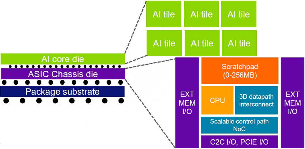
(Image courtesy eSilicon)
The blocks that go into either of these dice can be drawn from a library of what they call megacells and gigacells. The distinction between these two categories seems to go mostly according to how big the blocks are. As far as I can tell, there’s no actual “million” association with megacells, nor a “billion” association with gigacells. It’s just that gigacells are bigger than megacells. (I suppose they could have called them megacells and kilocells…)
Megacells include functions – largely mathematical – that might go into an AI tile. Examples include addition, matrix multiplication, pooling, convolution, and transposition. Gigacells, on the other hand, are larger blocks – like any of a variety of pre-configured AI tiles, network-on-chip (NoC) elements, processors, and I/O subsystems.
Turning a neural-net model into an executing block leverages the Chassis Builder, a design tool that eSilicon provides. The AI system comes together based on resources allocated from the libraries by the Estimator. (Note that the original green arrow from the Estimator to the chip is incorrect, per eSilicon; the arrow should go to the Executor instead, which then goes into silicon. The red X and new green line are my contribution…)
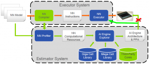
(Image courtesy eSilicon)
Not Your Grandfather’s RoI
This succession from software to ASIC has historically been followed in order to lower manufacturing costs – with performance playing second fiddle. In such cases, performance is a fundamental enabling parameter up to a point, so any implementation along the succession has to have adequate performance. More might be nice, of course, but, for a given application, once you have enough, well, you have enough. (“Enough” being a complex metric…)
Traditionally, you go down this path towards an ASIC both as a result of higher confidence – as your specific application proves itself in the market – and as higher volumes dictate lower costs. So any cost savings serve either higher profits or the need to drive pricing down and attract new business, consistent with the notion of price elasticity (assuming the application is indeed elastic).
But that’s not where the return on investment comes from here. These designs become accelerators that go into cloud facilities run by the behemoths that dominate the cloud. The faster they can run computations, the more jobs they can complete and, therefore, the more revenue they can gather. So this isn’t about reducing the cost of an accelerator board; it’s about performance – counter to the historical picture – and reducing operational costs. Here performance is king, and there is no such thing as “enough.”
So it’s a model different from what you might be used to, driving different priorities. You may be able to pay off higher accelerator board prices with increased throughput. All part of the math you need to run before you launch your design project.
With that, then, AI aficionados have yet another option for burnishing their AI story.
More info:


What do you think of eSilicon’s neuASIC approach?