

Looking to build some circuits that use light instead of electrons to make them super speedy? Well, you’re in good company, but you’d better buckle up: we’re still in early days on this stuff. All the pieces are there in concept, but we’re still figuring out how to integrate everything in a cost-effective, manufacturable manner. A recent IEDM conference paper pointed to one possible solution to a practical problem: getting a laser onto silicon.
To get started on this adventure, you need to bring together four critical components:
- A light source (aka “laser”)
- A way to carry light from one place to another (aka waveguide)
- Various gadgets that let you reflect and redirect light (Bragg gratings, adiabatic tapers and curves, couplers, etc.)
- Ways of detecting light to convert the information back into electronic form (aka photodetectors)
As we doggedly work to make everything smaller, it makes perfect sense to try to build all of this monolithically. But, if we’re going to do that, it would make a lot of sense to use the cheapest, most widely used materials and processes around; that would mean using silicon. Especially if we want to include CMOS circuits on the same chip.
And that, of course, is the idea underlying the notion of silicon photonics. You can build all of those things out of silicon – except for one: the laser. While silicon will happily move light from here to there via an obstacle course of photonic widgetry, it can’t generate the light itself. You need other materials – often III-V materials – to do that. It’s a direct vs. indirect bandgap thing.
So that kind of puts the kibosh on having a single rock (mono lithic – get it?) that can do everything for us and still meet the goals of using silicon in the first place (cost, integrated circuitry). So… if you can’t build the laser out of silicon, then can you attach a laser to the silicon and make something that is the next best thing to being purely monolithic?
The answer is, “Yes” – at least in concept. It’s referred to as a hybrid laser. But there are some gotchas that have only recently been surmounted by a team from STMicroelectronics, CEA-Leti, Univ. of Grenoble Alpes, and Vistec Electron Beam (and funded by the French national program “programme d’Investissements d’Avenir, IRT Nanoelec”) and presented at December’s IEDM conference. To see the big ideas at play, let’s back up and take a look at the two protagonists in this drama.
The first is the laser, which, for this project, was created using InP. For those of us not immersed in this stuff constantly, the laser is a stack of materials with p-type InP on top (a thick helping) and a thinner layer of n-type InP on the bottom. In the middle is a multiple-quantum-well (MQW) structure using InGaAsP. This involves several thin layers, the details of which weren’t covered in the paper.
I did some googling around to see what MQWs are typically made of, and they variously involve combinations of the III-V material with something else – in this case, InGaAsP. But how is it actually structured? Strangely, there’s precious little available online, other than vague references to “Material 1” and “Material 2,” or something similar.
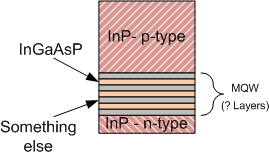
So I inquired with the team as to how their MQW was created. And, well, it turns out that MQWs aren’t simple, public things. They fall under the rubric of “special sauce,” and their details are not available. The response did allow a few clues: “I can say that we are using 2 [different] InGaAsP layers (with different In, Ga, As and P contents). This bi-layer is repeated several times (let’s say between 5 and 10 times) to form the MQW.”
Critically, the entire thing is about 3 µm tall. Yes, that is a tall feature in the context of a silicon wafer. We’ll come back to this in a moment.
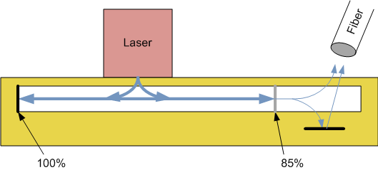
OK, so that was the laser part – the first protagonist. The non-laser part is what can be made out of silicon, and, in this project, it consisted of adiabatic tapers to take the light and transition it into the silicon waveguide (the adiabatic thing, as far as I can tell, meaning that you do it gently so that there’s no discontinuity or loss). Once in the waveguide, it could go in two directions (say left and right). Except that, mostly, they wanted to confine the light as part of the overall resonance thing. So, at both ends of the waveguide are reflectors that keep the light in place, bouncing back and forth.
Of course, if all the generated light stays in its little echo chamber, it doesn’t really do any good – you want at least some of the light to escape so that you can do useful things with it. So one of the mirrors is a partial mirror – around 85% – so that what escapes can be directed into an optical fiber. Some of that light is going to naturally go up in the direction of the fiber, but some of it is going to go down into the silicon, which is a waste. So they put a metal mirror underneath to reflect that fugitive light back into the fiber.
The following simplified image illustrates the basics of what’s going on here.
We’ll look at a more detailed view of how this comes together in a minute, but, before that, let’s get to the real problem here: how to attach that laser to the silicon. There’s a bit of a catch-22 that happens as you try to bond material from one wafer – the InP wafer in which the laser was built – and the silicon wafer. The surface for bonding has to be of very high quality – nice and smooth.
And that’s where the issue comes in. If you do this after you’ve done all your CMOS metal layers, you don’t have that nice clean surface. And the laser may be too far away from the silicon – that distance needs to be about 100 nm.
So if you can’t attach this thing after the metal is in place, then can you do it before the metal? Well, yeah, you can attach it, but then you’ve got this 3-µm skyscraper on the surface, which gets in the way of doing the metal steps after attachment.
What to do, what to do??
What this team decided to do was to attach the laser not to the topside of the die, but rather to the backside. That makes all of the metal shenanigans irrelevant. So the finished, more detailed structure looks like the following image. Those funny red squiggles indicate where the light is traveling.
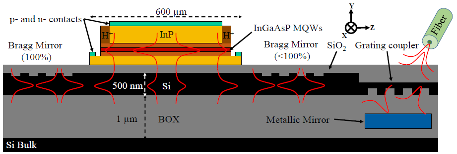
That “Si Bulk” layer isn’t from the SoI; it’s actually what remains of a silicon carrier.
(Image courtesy IEDM)
To be clear, this is done on SoI wafers. Most of the silicon features are formed first, and then a carrier wafer is bonded to the top. The whole thing is flipped over, and more processing is done to finish the silicon features.
Then the laser wafer – not really quite a laser yet, but the InP sandwich in wafer form – is bonded to the silicon wafer. (Which is a bit funky, since the silicon wafer is bigger than the InP wafer… but that’s a detail…) They then process the InP side by implanting H+ ions to create confinement on the sides of the laser and, through a series of etch steps, get rid of the extra material. The steps are illustrated in the following image from the paper.

(a) Build silicon structures and encase in SiO2; (b) bond Si carrier; (c) flip over and grind away SoI backside; (d) finish forming the Si features; (e) bond InP wafer; (f), (g) add H+ confinement, etch and add contacts; (h) metallize and encapsulate.
(Click to enlarge; image courtesy IEDM)
As far as they know, this is the first time anyone has done such a backside integration. It provides a way to get the laser right up in there where it needs to be while also remaining compatible with CMOS processing. While frontside application was often attempted with a pre-singulated laser, this is more efficient in bonding entire wafers – saving time and, presumably cost.
More info:
IEDM 2016 Proceedings, paper 22.2


What do you think of this way of attaching a III-V laser to silicon?