

At Semicon West this year, inspection seemed to be all the rage with two of the big equipment makers. Both KLA-Tencor (KT) and Applied Materials (AMAT) had new inspection stories, which we shall inspect today.
The motivator on all of them is – let’s see if you can guess this: complexity. Complexity and noise. Um, complexity, noise, and the increasingly tiny defects that now matter. OK, amongst the motivators are such diverse elements as complexity, noise, increasingly tiny defects, and an unmitigated desire to move wafers through the fab as quickly as possible.
KLA-Tencor Upgrades the Entire Team
We’ll start with KT, who announced six new systems. They’re based on existing brands, so there’s nothing completely new, but there are lots of improvements to address the need for better sensitivity, the need for a better signal-to-noise ratio (SNR), and the need for high throughput.
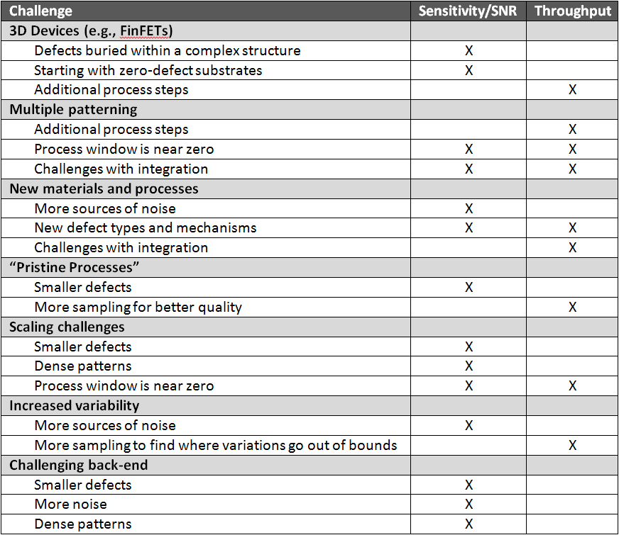
To illustrate the issues they were trying to address, they listed a number of areas of concern and the specific issues within each of those areas. These are illustrated in the following table.
Addressing these changes are a number of enhancements to their different families, which they group into two categories: the ones that do inspections – they figure out that something is wrong – and then the review stations where the wafers are sent when they earn detention – they figure out exactly what is wrong. (Hopefully.)
There are two aspects to the whole “finding the defects” thing. The first they call “discovery,” and it’s particularly useful with a new process or mask set: figuring out where the delicate parts of the design are. Kind of like figuring out which of the students are going to be trouble over the first couple days of school. The other piece is monitoring: keeping track of wafers in production so that you can see when equipment is starting to operate out of its designated parameters. Fixing such excursions as fast as possible is critical to ensuring that you don’t unwittingly misprocess large volumes of wafers.
The discovery machines are higher-end beasts, collecting and communicating large volumes of data for analysis. The monitoring systems have a delicate trade-off between sensitivity and throughput and cost, since they’re going to be employed during production, and you don’t want them to become the rate-limiting step. But you also want them not to miss defects. And you’ll need more of them, so they can’t break the bank.
The 3900 Series would now appear to be the flagship broadband pattern discovery family, along with the newest 2930 Series (which inherits the mantle from the 2920 Series). The 3900 trends toward the bluer end of the spectrum; the 2930 towards the red end. Both can leverage deep UV light for picking up tiny defects, but the 3900 has super-resolution for, well, better resolution. They have a chart showing the 2930 picking up defects down to 13 nm in size, with the 3900 picking up 7-nm defects.
KT indicates that the 2930 is also suitable for monitoring, so it would appear to straddle the discover/monitor line. Fully within the monitoring category are the Puma 9980, the CIRCL 5, and the SurfScan SP5. The first two are for patterned wafers, with the Puma system handling more or less straightforward optical inspection and the CIRCL having capability for inspecting, reviewing, and monitoring all surfaces of the wafer – including the edges. Yes, at today’s (or tomorrow’s) aggressive nodes, every spot on every part of the wafer could prove to be a clue to – or cause of – some problem.
The SurfScan series, meanwhile, is used for blank wafers.
Common amongst all of these systems is a focus on reducing noise, or what they call “nuisance” defects. These are, more or less, false positives and spurious signals. The new systems feature new algorithms to reduce the noise level, including a few “branded” technologies specifically for this purpose.
- The first is called “super-cell,” and it’s featured in the discovery systems. It treats N-type and P-type transistors separately, since they have different noise levels.
- The other two are similar – confusingly so (at least to this diletant). One is called NanoPoint, and the idea here is to focus on critical areas of the design identified in the design. This gives an early signal if mask tweaks are needed on a new chip in order to achieve proper yields. Part of this involves reducing the area of inspection to boost the defect-to-nuisance ratio. If you’re looking for a tiny defect in a 10-acre plot, the noise from 9.95 of those acres is going to swamp any actual signal. If you can identify critical square-foot areas to focus on, then you can much more easily extract a useful signal. NanoPoint has been around for a couple years on some systems; it is new to Puma with this release.
- The other similar technology is called “pin-point.” It is new on the broadband plasma systems (2930 and 3900), and it reduces the inspection area even further, again, for nuisance suppression.
What we’ve neglected thus far is the review part of the picture. This is where you know you have something amiss, but you have to figure out what. KT’s eDR7280 (up from the eDR7110) is an e-beam system with improved optical modes and performance, improved charge control (which we’ll see more of in a minute), faster setup, better classification, and the ability to communicate with the other inspection systems so that you can home in and identify issues more quickly.
Applied Materials Gets to 1 nm
Meanwhile, AMAT announced a new PROvision e-beam inspection (EBI) tool. And the story here is simple: they claim now to be the only EBI system able to resolve 1-nm defects. Yeah, those used to be noise, but not at the most aggressive process nodes.
And the defects with which they’re illustrating this are subtle FinFET issues – like bridges between fins or fins that have grown too big and are touching.
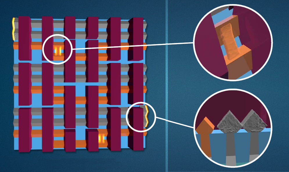
(Image courtesy Applied Materials)
The challenge they claim to have met involves achieving high resolution, which means a narrow column of electrons, all of which resent all of their neighbors. Cajoling or coercing them together more tightly is an important trick (and one of the many where the magician can’t reveal the secrets) – and all the while keeping the energy of the electrons “gentle” so that the little buggers don’t conduct their inspection with extreme prejudice, causing damage in the process.
However, making a higher-resolution small spot also reduces throughput because, at any given time, you’re looking at a smaller area, meaning you need more images to get the whole wafer done. So they’ve increased the current density, making for a faster read, and, ultimately, improving throughput such that it’s three times faster than alternatives – “for the most challenging e-beam applications.”
Note, however, that, unlike KT, AMAT isn’t targeting this e-beam machine at review; this is their hotspot inspection tool (more like KT’s 3900), making throughput that much more important.
More info:
KLA-Tencor Inspection portfolio


What do you think of these updated wafer inspection platforms?