

If you’ve ever digitized your vinyl albums, you know that you have a decision to make: what format should be used to store the music? There are lossless formats like wav and flac, but they take a lot more space. Mp3 is much friendlier to your small, limited-memory listening gadget, but you lose something in the translation. It’s lossy, so the space savings come at a price. Whaddaya gonna do?
Turns out that there’s a similar problem with chip test circuits. It’s not the only problem, but compression-vs.-loss is an issue that Cadence claims to have, well, not solved (it’s never completely solved until it’s lossless and small), but improved. As a result, they’ve announced a new Modus tool for this new approach to chip testing. (Yes, another tool name ending with “-us.” I just hope they don’t do a tool that flattens out hierarchy…)
Let’s start by reviewing. A long time ago, I wrote up the design-for-test (DfT) thing. Compression is a big part of it, because you want to decouple the number of pins used for test access from the number of scan chains internally. Ideally, you could have one pin per chain and load all the chains up in parallel, but that would require a crazy number of pins. You could also multiplex plain-text (so to speak) data from a few pins into the multiple scan chains, but that would require a lot of data and a lot of time.
So the answer is to apply compression. There’s a decompressor on the chip that takes the compressed pattern and delivers it to the scan chains. In the prior piece, I likened it to soft drinks: no one ships regular soda around – it’s too wasteful to ship all the water in the drink. Instead, they concentrate into syrup, adding water on location. Same thing here: the test data is compressed for transport until it gets into the chip, where it is diluted for your quaffing pleasure. (I know, I should be more consistent picking my analogies… soda or digitized LPs; they both work.)
The thing is that this compression isn’t lossless: the more you compress, the more you impact coverage. While more compression gives shorter chains, you need to add patterns to keep the coverage acceptable, and, eventually, the savings due to shorter chains and the extra time for more patterns cancel each other out. So compression has been, practically speaking, limited to about 100:1.
Cadence has summoned a 2D concept in this tool for a different problem – one we’ll come to in a minute – but it occurs to me that their solution to this compression limit also has a 2D character. Right now, each pattern entered spreads out laterally for loading. Every pattern is independent of the others. So thinking of a few pins expanding into many scan chains is kind of a 1D thing, where the data width is the dimension.
Cadence has added a time dimension to this: the compression engine now includes registers and feedback, so the history of patterns matters. The result is that you can get better coverage through this added dimension. Or, looked at another way, you can increase your compression ratio up to something like 400:1 or more without losing coverage.
They call this compression elastic. Before, all patterns were of the same length; now, pattern length will vary according to what’s necessary for coverage.
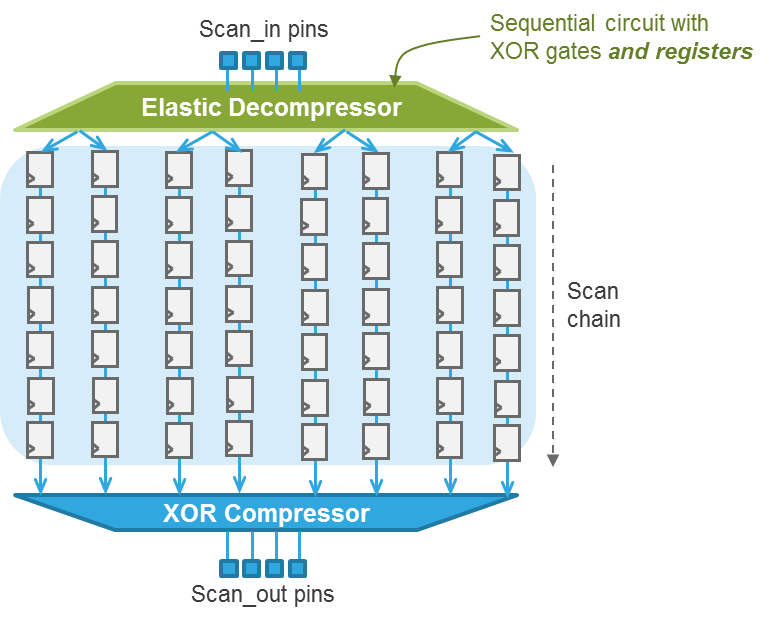
(Image courtesy Cadence.)
But that’s not all: there’s a second significant issue that has limited DfT, and some customers run into this problem before they hit the coverage wall. In the figure above, you see a single decompressor. And this is, in fact, how the thing has traditionally been built on a chip. So you have these scan chains all over the chip, and they all need to be routed to the “central” decompressor (and the compressor for generating the result).
Problems here can include congestion and wire length, depending on the size of the chip. Meaning that, yeah, for those monster chips, wire length will be a problem. Higher compression makes things worse because it increases the number of connections between XOR logic used for compression and the scan chains. They found that, in one example, 400:1 compression (which can now be done with decent coverage) chewed up about 10% of the routing resources. While more compression reduces chip testing cost, adding a ton of silicon adds that cost back in.
To solve this problem, they changed the compression math to allow the algorithm to be distributed throughout the chip, near the various scan chains. A gridded bus can remove the chaos inherent in getting input patterns and test results from and to the pins. They call this 2D compression because, well, the grid thing.
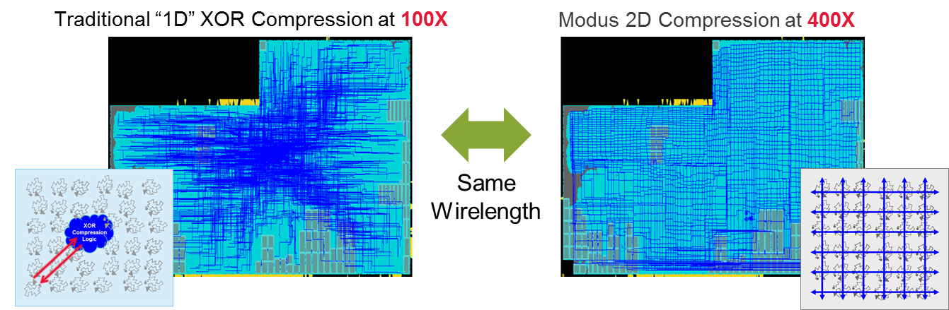
(Click image to enlarge. Image courtesy Cadence.)
Inserting this test logic into your design comes at the physical synthesis stage. While Modus is a separate tool from their Genus physical synthesis tool, they work together, so you wouldn’t be able to use Modus in someone else’s flow to mix and match tools and test strategy. You might be able to use a different place-and-route tool, except that you’d then be using one set of engines (timing, etc.) from Cadence for synthesis and another set from someone else for place-and-route, possibly slowing design closure.
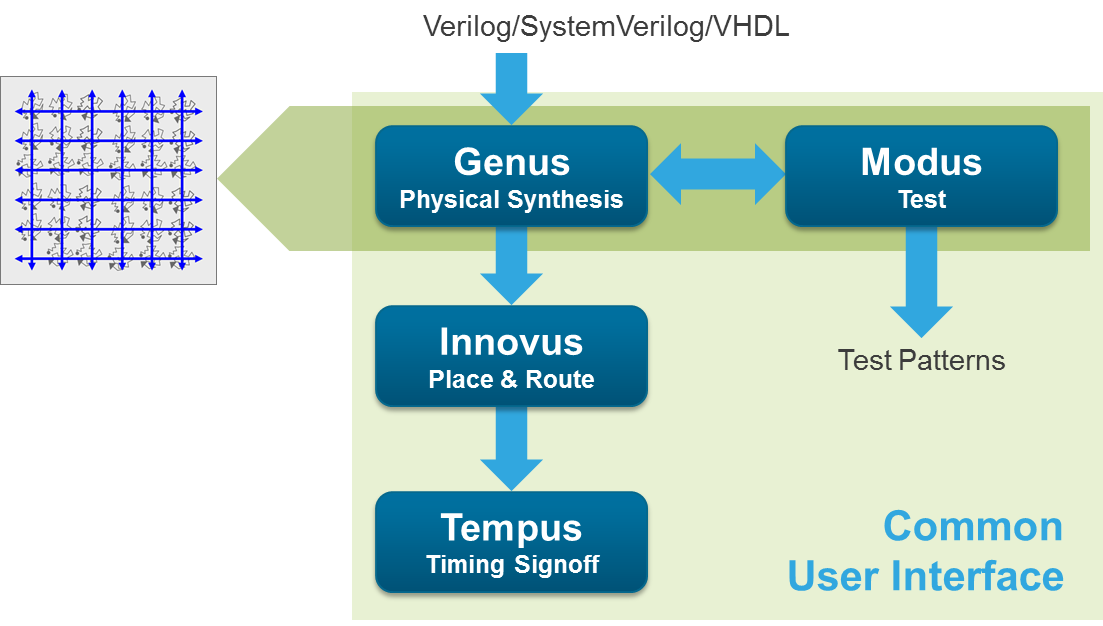
(Click image to enlarge. Image courtesy Cadence.)
The net-net impact of Modus is a 3X reduction in test time – oops, I mean a 67% reduction – and a reduction in wire length by whatever the inverse of 2.6 is (in other words, a 2.6X reduction… 62% for those who read critically).
There’s a bit more to the Modus story than elastic and 2D compression. They also modified their memory built-in self test (BIST) approach. Before, each memory needed its own BIST engine. Now all the memories can be placed on a single BIST bus, sharing a single engine and reducing the amount of silicon area dedicated to the BIST engines. But, better yet, it also improves memory performance during normal operation.
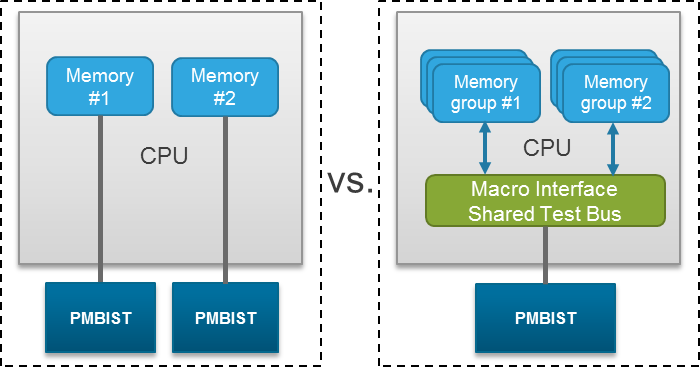
(Image courtesy Cadence.)
More info:


What do you think of Cadence’s new Modus DfT tool?