


Memory comes in many flavors. That’s because it’s used for so many different things, and requirements vary widely. We’re used to DRAMs, which we need to be able to get at often and quickly, and we’re used to FLASH, which needs to keep its contents after the power is turned off.
But there is other usage to be found on the other end of the volatility spectrum. At the far end is “one-time programmable” memory – OTP. For instance, if you use memory bits to store calibration information or to trim in some parameter, then, assuming you won’t have to account for aging in the future, you set it once and you’re done. You’ll never need to (or be able to) reprogram that again. Think antifuses and such.
Then there’s “few-time programmable” (FTP). This is memory that you may need to rewrite, but not very many times. Consider it OTP with an option. It will obviously have to be non-volatile, or else you’d be reprogramming on every power-up.
Who needs FTP? It’s perfect for code store, where you may need the occasional patch – but not on a daily basis. (Clearly, this wouldn’t work for Windows; after all these years, even Vista is still being updated frequently!)
We covered OTP, MTP (many-time programmable), and FTP memories way back in 2008. It was in the context of a company called Virage Logic; you may remember them. They were swallowed by another company you may have heard of: Synopsys.
Well, Synopsys recently released a new FTP cell. It shrinks the current FTP cell by a factor of 10-20.
Why are they worrying about this? Because we are experiencing much less segregation of technology these days. For all the benefits of integration, it brings with it some challenges. We used to have strict separation between analog, which had its own processes and dice; digital logic, where functionality was hard-coded into Boolean bits; processors; and memory – all the different sorts of memory.
Yeah, processors were (and are) made from digital logic, but they also require that most ethereal of technologies: software. At least you can touch hardware, and when it’s done, it’s done. Finito. Time to move along; the die is in the fab; no looking back now. Please.
Not so with software. You can never be sure what’s going to run. And, in particular, it’s never finished. You can run all the firmware you want to test out your processor before you cut masks, but it’s almost guaranteed that the firmware it will be running in five years – even five weeks – will be different.
But here’s the thing: this stuff is no longer separate. Digital logic and processors have been cohabitating for a good while, now. They’ve been combined with FLASH for code storage and SRAM (or even embedded DRAM) for working memory in microcontrollers for a long time.
Digitally controlled analog started the combination of digital and analog on a single substrate. And we’ve got analog interfaces (ADCs and DACs) on microcontrollers, so we see all four technologies combined together.
But even specialized analog chips – things that aren’t (or can’t be) integrated into microcontrollers, often involving power and higher voltages – are starting to incorporate processors that need code. And some of these technologies aren’t your plain-vanilla CMOS.
CMOS has traditionally been the ruler of all, the common denominator. When you talk about integration, the question is typically about whether some process – memory or MEMS or whatever –is compatible with CMOS. The CMOS is the bottom line, and everything else has to adapt – simply because CMOS is so prevalent and because so much cost optimization has been lavished on it.
So, being CMOS-compatible is a good thing, but there are other processes that merit consideration. For instance, BCD – no, not binary-coded decimal, but Bipolar-CMOS-DMOS – such as is used for higher-power analog chips. Bipolar for analog, CMOS for logic, and DMOS – double-diffused MOS – for high voltage.
Both BCD and, apparently, 5-V CMOS, are incapable of accommodating standard embedded FLASH technologies – at least not without modification, which increases costs. If you’re going to go the route of integrating microcontrollers onto such chips, you’ve got a memory problem to solve, given that you’ve got only two choices: standard FLASH, which is MTP, and FTP.
High-density FLASH uses so-called SONOS technology: silicon-oxide-nitride-oxide-silicon. It’s optimized for high density and low cost. Future FLASH is going all 3D, with stacks of films dozens deep and vertical shafts replacing horizontal layers for the storage cell. Very specialized stuff; not what you’re going to try to embed on a die with other non-memory stuff on it.
Meaning that an analog or other chip incorporating FLASH isn’t going to go in that direction. Then again, it doesn’t necessarily need to from a requirements standpoint: if it’s there to hold code, then it doesn’t need to be reprogrammed that many times. That is, unless your software development process is completely hosed, in which case you’ve got bigger problems. Let’s assume you’re better than that.
Then there’s Synopsys’s existing FTP block. Problem is, the bit cell was too big – or, rather, bigger than it had to be – as they proved by developing the recently-announced alternative that cut the area by 90-95%. It programs via hot-electron injection and erases by Fowler-Nordheim tunneling, so it’s basically FLASH. Even with the size reduction, however, it doesn’t compete with the cost of SONOS for super-high densities, so they don’t see the cell migrating outside of these embedded applications.
Instead, they’re occupying a “sweet spot” in density – what they’re calling “medium density.” The cell is intended for memories up to 64K bytes. The endurance – the number of times the cell can be reprogrammed and still maintain the specified data retention – is 1000. You’ve got that many opportunities to update your code.
Looking back on my early coverage of MTP and FTP, this actually lies somewhere between the two. At that time, I wrote of MTP requiring 100,000+ cycles; FTP was 10s to 100s of cycles. Synopsys appears to be referring to their new cell as MTP, but it’s clearly on the low end of the MPT scale. Realistically, it’s still “a few times” reprogrammable.
Much of their publicity focus is on the bit cell itself; after all, that’s where the big area reduction came from. But the overall IP needs more than that, since there are a couple of complicated aspects to FLASH technologies.
One is the high voltages that the cell requires for programming, along with what have historically been complex algorithms for ensuring that cells aren’t over-programmed. In fact, in the early days of FLASH, those were things that system designers had to pay attention to. But they’ve long been abstracted by the FLASH makers: they take care of the details, saving significant design hassle. And that’s the case with Synopsys’s new MTP IP: the charge pumps and programming logic are included. They also use error correction for increased reliability.
The second complication can be of particular import when you don’t have unlimited programming cycles. Let’s say that your code fills only half of the memory; you’ve saved the rest for headroom for upgrades. If each update reuses the same memory cells, then, after 1000 updates, the bottom half of your memory will be used up – even though the top half hasn’t been touched. (Assuming your updates in fact did not grow in size like you thought they might).
In an ideal case, if you used no more than half the cells, then with each update, you could swap which half you programmed – and get 2000 updates as a result. If you used only 1/3 of the memory, then you could triple the endurance by moving to a different third with each update.
This concept is called “wear leveling,” and it involves complex algorithms that ensure that all bits in the memory get a reasonable chance of being used. If you’re updating code that used to reside at address 50, it will likely not be placed at address 50 when updated; it will go somewhere else. Which means that you need a translation layer to turn the address as presented at the external pins into whatever the current location of cells is.
However, although the endurance on these cells is 1000, the actual number of times that Synopsys expects users to reprogram is in the 10s or maybe 100s – the classic FTP realm. That means that the endurance already provides as much as an order of magnitude more reprogramming cycles than will likely be needed, so they have foregone the extra expense of wear leveling. If it were important for a given application, then a designer could wrap some wear-leveling logic around it – being app-specific, it could probably be simpler than a universal solution would have to be.
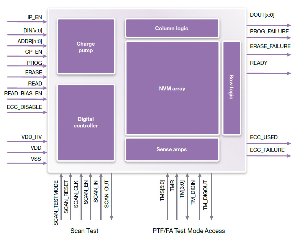
Image courtesy Synopsys
So technologies that have had to rely on external memories before can now integrate non-volatile memory. Automotive is a big target application for this, although it’s not for “grade 0” use, under the hood, where lives may be at stake. Synopsys says it’s good for grade 1 or 2 – things like the center stack, infotainment, seat position memories, automatic door sliders, and the like. (Although, if Hollywood is to be believed, sliding van doors can be quite dangerous. And maybe we’ll have some future horror show where some nameless entity hacks the seat system and forces the driver ever forward until…)
Not only is the cell compatible with these processes, but it can be implemented with no changes to the processes – no extra mask layers or films, reducing costs by as much as 25%. Looks like BCD and 5-V CMOS have earned parity status with traditional CMOS.
More info:
Synopsys DesignWare Medium-Density NVM


Do you have applications for a memory like Sysnopsys’s new few-time programmable NVM?