


So your company needs to design a system-on-chip (SoC). On the one hand, there’s a lot of that going around. On the other hand, the cost of doing an SoC – especially on an aggressive silicon node – is so expensive that the number of companies that have the cash to do that is decreasing.
Which limits the number of competitors to a certain degree. But you’re still going to have competitors. How are you going to make sure that, when system builders are looking for an SoC, they choose yours?
That’s how a standard product marketing discussion might go, but things can work differently with SoCs, While you might find merchant-market SoCs for, say, a communications protocol like Bluetooth or for power management, many SoCs are created by, or on spec for, system builders, so presumably the feature set has been tuned to be exactly what the system needs. So, really, it’s the system architects that are defining the differentiating aspects of the system, and the SoC is “merely” an implementation of those features.
Which would suggest that the SoC itself has less impact on the success of the system. But if the features themselves aren’t a hallmark of the SoC, the usual real-world impact of the SoC is enormously relevant: How fast does it go? How quickly will it drain your battery (or brown out your town)? And will it support the economics of a profitable system?
And then there’s the other biggie: did you get the chip out fast enough to grab that early chunk of the market?
According to Invionics, this exposes competition on a different level. It’s not about the bells and whistles on your product: it’s about your SoC design process. The general idea is that companies that are more competent at IC design will have more competitive products.
Invionics is an EDA startup, but, unlike most EDA startups, it’s not trying to compete directly with the Big EDA Guys. And it’s not trying to outdo something the Big Guys already do in the hopes that one of the Big Guys will buy them. (They still might want a Big Guy to buy them; I have no idea. But that’s neither here nor there for our purposes – the point is orthogonality.)
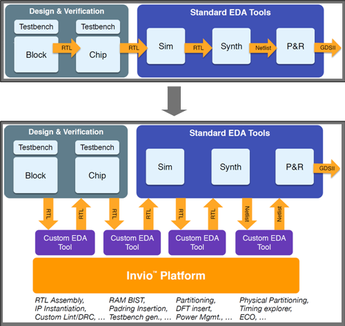
Their basic thesis is that standard EDA flows are starting to look alike. If everyone simply goes through that flow, then everyone will pretty much get the same result. This makes it harder for companies to compete at the IC level.
But, they note, IC designers have lots of ideas on how to improve on standard EDA tool results. Or how to speed up the process through automation.
You’d think that such designers might want to work closely with their EDA partners to work those ideas and priorities into new releases of the tools. But, actually, no, they don’t. Because if they did, then their competitors would also benefit from these great ideas. New ideas to boost competitiveness aren’t so effective if you hand-deliver them to your competition.
You want to be able to perform your tricks, but you want to keep it in-house. So each engineer writes a specific custom script, unaware that four or five other designers in the company are writing the same script (only differently).
This is the problem that Invionics is trying to solve with their new Invio EDA-customizing platform.* Their solution keys on the fact that modern EDA tools leverage open design and verification databases (for the most part). Clever designers know how to get into those databases to check or modify parts of the design outside the main flow.
But such mucking about comes with a lot of work and with some risk.
- If you’re looking for specific design constructs, for example, then you have to be able to parse the design language in order to make sense of anything coming back. And you may be working with multiple languages.
- If you’re making design changes, you’d better make sure your script isn’t creating any surprise syntax problems that you’re going to have to untangle later.
- Even if your syntax is good, are there knock-on effects that you haven’t anticipated? Did you solve one problem, but inadvertently create a new one?
The thing is, many such scripts focus on one specific task. And there’s always the tradeoff between the time you’re going to save with the script and the time it takes to create the script. And the more you test it out, or the more time you have to spend fixing the problem that arose when you fixed the earlier problem which was caused by your original script, or the fancier or more intelligent you make the script, the longer it takes to finish, and, at some point, you’ve lost your edge.
What Invionics proposes to do is to let you and your company take those best practices, those tricks and shortcuts that you believe give you an edge, and create custom applications for getting them done. They interface into the design and verification databases, handling the parsing and interpretation of data and keeping track of the relationships and dependencies between entities.
They’ve done a few things to allow you to treat this as a script, but with features and robustness that would be really hard for you to create ad hoc (and still stay on schedule).
- The scripting is still done in Tcl or Python, so it should be familiar.
- It can handle Verilog (digital and AMS), SystemVerilog (synthesizable or not), UVM, and VHDL.
- Its API is language-agnostic, so you don’t need to change your script if you reuse the application on a different design done in a different language.
- It has specific modules for:
- RTL (behavioral) modification,
- Netlist (structural) modification,
- Verification, and
- SoC assembly.
But there are two additional capabilities that can be big productivity enhancers. First is a GUI package. Yes, I understand, it’s exceedingly manly to design using cryptic command-line interfaces, tossing out low-level calls and long parameter strings like a boss. GUIs have seen better success in hardware design than they have in software design, but, although the main tools may be heavily GUI-oriented, scripting has been less so.
Well, now your script can operate with a GUI, replacing strings of obtuse commands with a click of a few buttons. The GUI package comes with your standard collection of widgets so that you should be able to slap them down quickly and get on with life.
And there’s one other productivity feature: you can package your flashy new custom EDA adjunct tool as an executable, making it available throughout the company. Make once, use many.
The assumption is that you’re going to continue to use the big tools you’ve invested in from the Big Guys; that’s not going to change. But instead of simply living with what they give you as you move from early RTL to finished design, you can drop out at numerous places, using your own tools to customize that flow.
(Image components courtesy Invionics.)
Does this mean the end of flashes of inspiration by the lone maverick designer who’s going his or her own way, convinced of the righteousness of the ronin? Well, not necessarily. That same designer can use Invio to develop that one-script-to-rule-them-all more quickly.
That said, there is a sense that, with a little benevolent management, a company could take more centralized ownership of these compete-critical processes, making them available to more folks while reducing the amount of time designers have to spend creating such tools. A balancing act to be sure. Central management doesn’t preclude the occasional well-placed individual effort.
If Invio works as promised, then these little acts of scripting can change from tactical tools to strategic scripts, encapsulating and formalizing the secret knowledge that sets your company apart.
*A note on pronunciation – it’s a tad confusing. They pronounce “Invionics” with a long middle I: “in-vie-onics” (the “vie” rhyming with “eye”). But the product name has a “foreign” I (equivalent to English long E): “in-vee-oh.”
More info:


Do you see a benefit to creating new custom tools using a platform like Invio?