System on Chip (SoC) design today is an incredibly complicated collaborative endeavor. By applying the label “System” to the chips we design, we enter a realm of complex, interdisciplinary interactions that span realms like analog, digital, communications, semiconductor process, and – with increasing dominance – software.
Since the first SoCs rolled out a mere decade or so ago, the composition of design teams has shifted notably, with the percentage of cubicles occupied by software developers increasing much more rapidly than those of any of the other engineering disciplines. In most SoC projects today, software development is the critical path, and the other components of the project are merely speed bumps in the software development spiral.
With that in mind, it is essential that we start the software development phase of our project as early as possible, and then do everything we can to keep those programmers productive and happy for the entire duration of our project. Beyond the time-honored tradition of slipping pizza under the door, one of the best ways to get programmer productivity up is to provide a prototyping environment where programmers can get started early, rather than waiting for tapeout to begin the long, arduous process of swatting all the configuration-specific bugs that are bound to plague our particular SoC hardware architecture.
FPGAs have been the go-to technology in the quest to build working prototypes suitable for software development and debug. FPGA companies have created a special category of devices specifically tailored to the needs of prototypes. Numerous companies build gigantic prototyping boards with various arrangements of FPGAs, interfaces, and nifty tricks aimed at smoothing out the arduous process of creating and bringing up an FPGA-based prototype.
From the hardware design perspective, the FPGA-based prototype is just the last in a sequence of virtual and real prototypes we use to debug and validate our system before we go to tapeout and final production. Most teams use simulation and software-based virtual prototypes for the early-phase validation, then move on to big-iron emulation for in-depth hardware debugging, and then finally to FPGA-based prototypes for software development and debug and final validation of the hardware design. With the FPGA prototype usually coming last, the time to bring up the FPGA prototype (and therefore open the door for real software development) is a critical element in SoC project schedules.
Many companies persist in building their own FPGA prototypes from scratch. This makes sense in some situations, such as where the project is a simple evolution of a previous project for which a home-grown FPGA prototype was already built. For anything without a legacy prototype, however, building from scratch is a complicated, time-consuming design project – situated at exactly the wrong phase of the overall SoC development schedule. For that reason, many teams go with commercial prototyping boards or systems, where the hard work of board design and integration are already done, and where (presumably) other teams have shaken most of the bugs out of the platform itself.
Even starting with a commercial prototyping board or system, however, the complexity of bringing up a prototype can be daunting. The gap between your working emulation or simulation model of your design and the one you envision purring away on your FPGA boards is huge. Often, commercial prototyping boards are just that – boards – without the software and IP support you need to get your non-FPGA design up and running on a bunch of interconnected FPGAs.
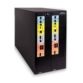
Cadence just announced what they call their “Protium” FPGA-based prototyping system – aimed at taming many of the common issues with the bring-up of FPGA-based prototypes. Cadence says the new platform targets the mobile, consumer, networking, and storage segments or, to put it another way, just about everybody who designs SoCs. Protium is based on the current biggest, baddest, prototyping-specific FPGA – the Xilinx Virtex-7 2000T. These 28nm interposer-based FPGAs pack around 2 million 4-input LUT (equivalents) into each device, so it doesn’t take too many FPGAs to create a very large prototype. The advantage of such large FPGAs is a dramatic simplification of the process of partitioning your design into FPGA-sized chunks and managing the communication and interfaces between them. Cadence says that the new platform packs 4x the capacity of their previous offering – up to a claimed capacity of 100 million gates – probably largely on the shoulders of the new, bigger FPGAs.
There are a number of V2000T platforms on the market, however, so the FPGAs alone don’t particularly distinguish Cadence’s solution. For real differentiation, we need to look at the compatibility with the rest of Cadence’s “System Development Suite.” For design teams already using Cadence’s Palladium, for example, Protium brings big value by sharing the bring-up flow with the popular Palladium emulator, which Cadence claims reduces the bring-up time by as much as 70%. Cadence says this 70% represents an improvement from “months” to “weeks” for a typical FPGA-based SoC prototype.
Typically, when bringing up a prototype, we first have to deal with importing and re-synthesizing our HDL design with the FPGA-based target. This means dealing with a completely different “FPGA-style” clocking scheme, portioning into multiple FPGAs, handling IP, morphing our memory architecture into something supported by the FPGA platform, and dealing with a range of smaller FPGA-isms that creep up. By sharing a flow with Palladium, Protium at least shares the cost and effort of overcoming most of those obstacles across two project phases. Protium automates memory compilation and external memory support, so taming the memory beast should be significantly easier. Protium also preserves the naming of your RTL objects throughout the flow, so when you do encounter a problem, the task of tracing the bug back to your RTL source should be significantly easier.
Cadence also packed a powerful clock transformation capability into Protium, separating your design from some of the ugly realities of the FPGA world. Your source design can contain an unlimited number of user clocks, so you’re not constrained to the FPGA limits. The transformation also handles traditional FPGA shortcomings like gated clocks, latches, and internal tri-states automatically. Cadence claims it will also eliminate hold-time violations that often result from transformation of clocking schemes into the FPGA domain.
On the seams between FPGA partitions, Protium’s compiler automatically decides whether single-ended IO or LVDS will give the best performance, and it automatically generates all of the constraints and switches for FPGA place-and-route. In addition to reducing the overall effort, this should mean quite a bit less time for the team to become “expert” enough with the FPGA-specific tools to complete the job at hand.
When it comes time to debug, Protium has a rich set of features including real-time monitoring of pre-defined signals, force/release of signals to specified values at runtime, internal memory upload and download, logic analyzer-like probes, start/stop clock, and waveform viewing that spans multiple FPGA partitions. This lets you work in your “overall design” space rather than in a “single FPGA space” as you’re debugging.
Protium promises to be one of the most turnkey prototyping solutions on the market, and it should offer compelling advantages over stand-alone commercial prototyping boards for a broad range of customers – particularly those who already use a Cadence flow for the rest of their design. As SoC design continues to grow in complexity, and as software development and debug expand to occupy more of that complexity, the value of FPGA-based prototypes will only increase.