


Security wonks talk about the “root of trust” for computer systems, and for good reason. If you can’t start from a known-good position, everything that happens afterwards is potentially suspect. Building castles on sand, and all that.
Since every computer and embedded system has to bootstrap itself from cold metal, the boot-up process is necessarily the root of all subsequent trust. If the boot ROM is compromised… well, there’s no telling what mischief may follow.
That’s the concept behind Microsemi’s new “secure boot reference design.” Lock down the bootstrapping process first, and you can then start building a secure system on top of it. A lot of companies have made token efforts to secure their respective processors’ firmware. Encryption, anti-hacking measures, obfuscation, and so forth. But Microsemi is different in three ways. First, it’s much more complete (and paranoid) than any other approach I’ve seen. Second, it secures other vendors’ processors, not its own. And finally, it’s not even a new chip – it’s programming for existing devices.
The details of Microsemi’s scheme are necessarily intricate and arcane, but the overall concept is simple enough: prevent the contents of the boot ROM from being corrupted, and make sure that only good code reaches the processor. Once the CPU is on its feet, turn over control to somebody else’s code, at which point further security becomes someone else’s problem. Microsemi can’t guarantee that your Linux drivers haven’t been hacked, but by golly, the system will be pure and uncontaminated when they’re loaded.
So how’s it work? Basically, by inserting a chip between your processor and its boot ROM. Specifically, it relies on one of Microsemi’s SmartFusion2 FPGA/CPU combo chips. You remember SmartFusion2. Back when the company was still called Actel, it announced a new family of chips that combined an ARM Cortex-M3 processor, programmable logic, and flexible analog components all into one programmable system-on-a-chip. In some cases, a single SmartFusion2 might be all the hardware you need. In this case, it’s an intermediary – a man in the middle – between your processor and your boot code.
Assuming your CPU talks to its boot ROM over SPI (a requirement of the current reference design), you simply snip the connection, plant the SmartFusion2 device in its place, and reconnect the boot ROM on the other side. Voila! You’ve turned a simple four-wire interface into a smart, security-managed, intelligent, programmable, bootloader watchdog.
That’s the easy part. The hard parts are figuring out whether the boot image is genuine; transferring that code to the processor without allowing it to be intercepted or corrupted; and making the processor execute boot code that’s been encrypted.
The magic wand you want to wave over this whole process is generically known as white-box cryptography (WBC). Here, “white box” refers to the easily accessible nature of the hardware, as opposed to a closed “black box.” To ensure the maximum level of security, we have to assume the worst: that attackers will have total physical access to the embedded system and that they are able to trace, measure, probe, disassemble, cut, or solder anything they want. The trick then becomes engineering security measures for a system that’s wide open to reverse engineering.
The first step is to never transmit a cryptographic key in the clear. Fine, but how do you do that when all your software is transported over SPI? It’s pretty easy for the bad guys to monitor an SPI bus and disassemble all the code, or to inject malicious code over the same SPI bus.
Part of the solution is to bury the crypto keys in amongst the bit stream of the software itself, and this is where Microsemi’s SmartFusion2 device comes into play. It uses uninitialized SRAM cells to harvest a few thousand random bits of random data, seed a key with it, and use that to encrypt and obfuscate the “real” key as it makes its way to the host processor. Because the SRAM noise is different every time the system powers up, this initial one-time key, or nonce, changes every time.
It would have been easy enough for Microsemi to just encrypt all the boot code and send that to the processor, but most processors can’t execute encrypted code. So it does the next best thing by sending the boot code in plaintext, along with the obfuscated AES key and the SRAM-seeded nonce. That allows the host processor to authenticate the boot loader without having to decrypt the whole thing or to share a hard-coded or permanent key with SmartFusion2.
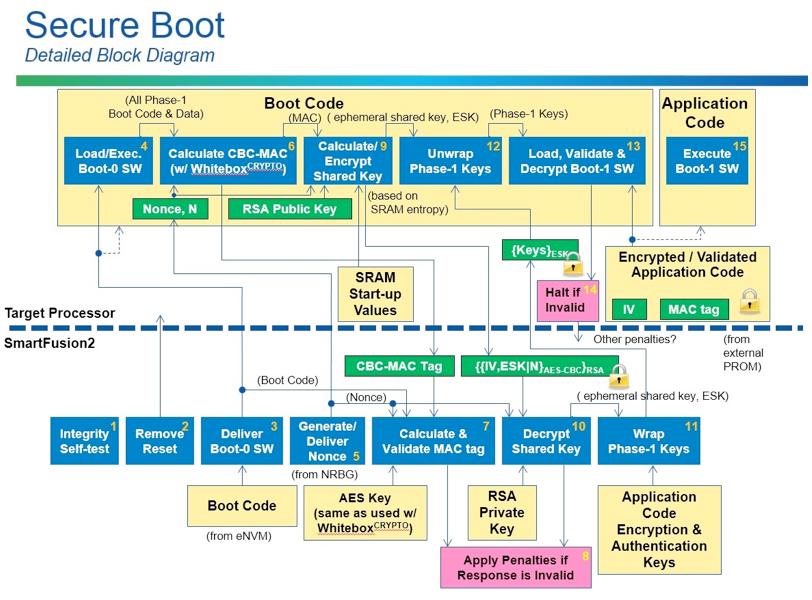
The processor and SmartFusion2 then both generate and share another set of keys, which are used to protect the transport of the larger application code. Sound complicated? You betcha. But Microsemi has done all the work. All you have to do is buy it.
The company says its secure-boot design will work with even the smallest and cheapest SmartFusion2 device, so you’re looking at about $7 in additional hardware cost. If you’re already a SmartFusion2 customer, you might get lucky and be able squeeze the new logic into an unused corner of the device, making the security features essentially free.
The encryption key is going to cost you, however. Microsemi sells single WBC keys for $11,500 a pop, or a program to generate unlimited keys for $95,000. That may sound like a lot of money, but if you’re making high-reliability equipment, it’s probably a drop in the development-project bucket.
As we saw recently, embedded systems are increasingly coming under attack, partly because there’s more of them, and partly because they’re becoming more interesting to attackers. Sooner or later, we’ll all have to secure our designs, starting with the boot process. Internal boot ROMs can help a lot, but, for systems that load code from external storage, Microsemi’s elaborate man-in-the-middle approach looks likely to keep the bad guys at bay.


