


We recently took a look at Lattice’s approach to sensor hubs. We’ve seen many other ways of implementing sensor hubs in the past, but all of those were software-based; it was just a question of where the software executes. Lattice’s approach is hardware, and that raises all kinds of new questions.
The biggest red flag that it raises for me is that moving a task from software to hardware in the design phase is not trivial. (Trying to keep it with the software guys, using tools that automatically generate hardware is, for the most part, a quixotic goal that seems largely to have been lovingly placed back on the shelf.) In my quest to figure this part out, I found that there’s more to the sensor hub world than all-software and all-hardware. And that makes the design question even more complex.
So for the next couple of pages, I want first to explore some of these different sensor hub designs; after that we’ll go into the design flow implications. In the final analysis, from an architectural standpoint, this is a partitioning question. I suppose that, by definition, a sensor hub in and of itself is the result of partitioning software out of the AP, but now it’s more than mere software partitioning: it’s software/hardware partitioning.
Because I’ve already covered them, I’m not going to delve deeper into the all-software and all-hardware approaches until we return to the design flow question. What’s of interest at this point are two alternative architectures available on the market today: one from PNI Sensors and one from QuickLogic. We’ve covered them both at a high level before, so here we will dig in further to understand how they’re split up.
How the heck do I build that?
It’s worth mentioning that all sensor processing, to some level, involves hardware. As pointed out by Movea’s Bob Whyte, the ASIC that accompanies most sensors will handle the low-level A-to-D conversion, calibration, decimation, and serialization for delivery onto a bus. The functions we’ll be describing are at a higher level than these, and, critically, they affect the fusing of multiple sensors rather than simply the processing of a single sensor’s data.
At this higher level, the decision about what goes into hardware and what goes into software is a classic one. Hardware typically provides much higher performance and, usually, lower power (garden-variety programmable logic being the exception here). Software provides flexibility and, sometimes, lower cost, since you use one piece of hardware (the processor) for everything rather than creating custom logic for each custom function. Those custom functions can chew up silicon real estate, especially if pipelining and replication are needed to boost performance.
Using the processor for everything works only if the different functions can execute at different times. If they have to be completely concurrent, then you need to use either multiple processors or hardware. The functions we’re describing here don’t fit into that category, so concurrency per se is not a critical issue.*
The hardware options we’ll discuss are either full-up custom hardware or programmable devices that have been specifically optimized for this role. So we can assume that hardware – programmable or not – will be faster and lower power; software will be flexible.
Cost? Well, I’m not going to get into that. The system developer’s cost for a solution may not be the solution provider’s cost. There’s the matter of “price to value, not to cost,” and the difference is profit. So there may be some high-priced-but-low-cost solutions. I haven’t seen any teardowns, so I’m going to omit cost from the discussion. I know… spoken like a true engineer.
That leaves us with flexibility vs. power/performance. Simple. When do you need flexibility? In our context, you need it when you anticipate change in the algorithms. Those changes might even need to be applied to systems deployed in the field, but, at the very least, you need to mitigate how many different hardware designs you have to do.
Even if your customers never update their sensor hubs in the field, your algorithms will likely improve over the next couple of years, so you might change the content of what you ship every 3 or 6 months. You don’t want to be doing a hardware change that frequently; masks are too danged expensive for that. FPGAs bring back some of that flexibility, although the design flow implications that we’ll discuss shortly mean that this can’t be taken for granted. For our purposes, then, I’m going to consider FPGAs to be semi-flexible.
So the partitioning question becomes: which stable portions benefit from the performance and power of hardware, and which portions are likely to change in the future? I noted in the past that sensor fusion algorithms seemed to be making a change from consisting largely of math for calculating things like quaternions to being much more heuristic in nature. Math can be pretty firmly decided; heuristics, by their very nature, aren’t so precise.
So an obvious partition is to do the math in hardware and keep the heuristics and other fuzzy stuff in software. This is specifically what PNI Sensors does in their SENtral sensor hub chip. This device, whose content is not user-programmable (with the exception of a few key parameters stored in registers), contains both hardware and software. Each of the math functions that they’ve hardened executes in a single cycle. They use an ARC processor for the portions they keep in software.
This use of a processor with a customizable instruction set is not unique or surprising. When power is the enemy, cycles are evil. So you want to do as much as possible in each cycle. Then you can ratchet the clock speed down; the SENtral device runs with a 10 MHz clock (compared to 150+ MHz for a typical microcontroller). They further keep power down by using ROM rather than RAM (at the expense of some flexibility, of course). The other benefit to custom CISC is fewer instruction fetches; this further reduces power.
QuickLogic’s solution is more nuanced yet. They have 1000 logic cells to use for everything; that’s not much. They say that a 32×32 multiplier can swallow that many cells, and, with sensor fusion, you’re not doing just multiplication; you’re doing matrix multiplication. So how do you make that work?
They build a single multiplier out of hard gates, time-multiplexing and sharing it for the various computations. This is managed by a micro-coded state machine.
Then, in addition to this, two custom-instruction CISC processors are laid down. These are like ARC or Tensilica processors, but they aren’t specifically ARC or Tensilica. One processor manages the sensors, polling every 20 ms and storing the data. The other processor grabs the stored data and handles the fusion algorithms.
The sensor polling is done serially; the polling rate may depend on the type of sensors involved. Some, like temperature and humidity sensors, sample phenomena that change slowly, and so these can be polled less often. Motion-oriented sensors, on the other hand, would need more frequent check-ins.
The clock frequency they use is low: 30 kHz. Yes, that’s with a “k”. If more sensors are used than can be polled serially at that frequency, it might have to be raised a bit.
I guess this is as good a place as any to make note here of something I’ve said elsewhere that turns out not to be correct. I’ve said that multicore hasn’t been used in software implementations. Clearly that’s not correct, since the QuickLogic solution has a micro-coded state machine and two CISC processors running in parallel. This isn’t done so much for needed concurrency as it is a way of decomposing the problem to manage complexity.
Of course, there is only so much fusion that can be done in the CISC processor. So, where QuickLogic perceives that they’ve left the domain of simple fusion and entered the more complex domain of context, then they defer to the AP for that. In order to keep from running the AP too hard, they rely on the notion that context – if it means “what’s generally going on right now” tends to change slowly, so they feed the AP new data every fifteen minutes or so. That gives the AP time to sleep if nothing else is going on.
So now we have four sensor hub variants, summarized in Figure 1:
- Traditional software implemented in a microcontroller, which may be external or collocated with the sensor;
- QuickLogic; part fixed hardware, part programmable hardware, part microcode, part software;
- PNI Sensor: part fixed hardware, part “fixed” software (with register settings);
- Lattice: all programmable hardware.
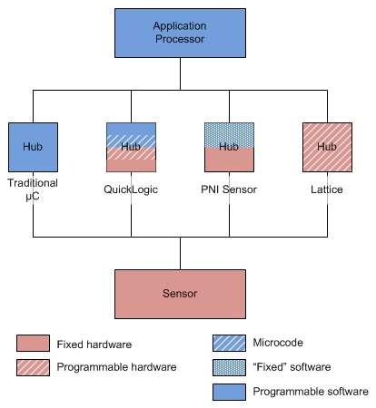
Figure 1. Sensor hub hardware/software partitioning options.
How the heck do I design with that?
Now, given these very different ways of approaching a sensor hub, how is a user of these devices supposed to implement an algorithm? There are a few different angles here.
Let’s start with the traditional microcontroller hub. Fusion algorithms tend to start at a high level, created by an algorithm jockey using tools like Matlab. Matlab creates “science” code that then has to be turned into real-world “engineering” code for running on a specific processor in a specific system.
That process is easiest if the system implementation is software-oriented. That doesn’t mean that there’s no work to be done; these microcontrollers are small, and algorithms have to run using as little power as possible. So there’s lots of optimization and code rewriting that may be necessary. Bloatware need not apply. But… it’s a software problem, turning generic code into specific code. Nothing surprising.
Also relatively straightforward is the PNI Sensor solution, for an entirely different reason: its functionality is fixed, save the possible setting of a few register values. They say that they spent a lot of time optimizing their hardware and software, so if their customers were able to change the functions, the work would not be trivial.
Next in the complexity scale is the Lattice solution. This isn’t so much a question of difficulty as it is one of effort and design culture. First off, the input is software and the output is hardware. Yes, there are tools like Calypto’s Catapult C that can help to convert untimed C code into an RTL hardware language, but it’s work, and it’s not trivial or cheap. It’s entirely likely that the project will be a full-up hardware design done without any tool assist. That means hardware engineers; specifically, FPGA designers. Even if you use a tool, it’s still a hardware project.
That conversion process adds time to the design schedule. Now, software tends to have the benefit of being able to come dashing to the train right as the door is closing, tracking toilet paper on its shoe, and still manage to make it on board as the product is released. Heck, someone can even toss a few bags in the window after the train is moving. That’s not the hardware culture.
Yes, Lattice’s device is programmable, so last-minute – or in-field – changes are possible. But, while adding or moving a few software instructions around in a software program is usually no big deal, it’s very hard to know what might be a big deal if the FPGA content changes. What might look like a trivial algorithm change in software could turn into a nasty change in hardware – especially once the pins have been fixed.
That’s not to say it can’t be done; it’s just that – well, have any of you tried to use Microsoft Word as a page layout tool? Something it was never really designed to do well? You know, with drawing frames flowing text and such? You get the page looking exactly the way you want it and then make a miniscule change, and suddenly drawings are snapping to all kinds of weird places you never intended, and now you spend a half hour trying to establish a new stable page layout that includes the trivial change that caused so much chaos. I don’t want to insult FPGAs by comparing them to Microsoft software, but you get the picture: Seemingly minor tweaks can cause major headaches. So hardware programmability isn’t as forgiving as software programmability. Hence my “semi-flexible” designation above.
The other big open question is, how much sensor fusion will fit in one of the Lattice devices? They’re exceedingly small-footprint, low-power devices, but it has yet to be proven what can be done. Granted, they have more LEs than the QuickLogic device (ignoring the multipliers – yeah, I know, that’s not really fair), but you can see the kinds of tricks that QuickLogic had to do to implement fusion in their device. That’s no software-to-hardware rote conversion; it involves a carefully-crafted low-level micro-architecture. And I have to say that I came away from my QuickLogic conversation feeling like they had really thought the problems through in great detail. Perhaps the extra LEs in the Lattice device make such acrobatics less necessary, but time will be needed to prove out the number of gates required.
Finally, we look at the design process for users of the QuickLogic device. Even though their chip is built using FPGA technology, it is not positioned as an FPGA; it’s a customizable sensor hub. So what does that mean? At the simplest level, it comes with some canned sensor fusion algorithms that were done by Sensor Platforms. Little more is needed if you’re satisfied with the functions it provides:
- context awareness (presumably at a limited level, since they say they push most context to the AP),
- step count,
- magnetometer diversity, and
- buffering
Beyond that, there’s a custom tool that lets the user specify the sensors and algorithms to be used. That’s all well and good, but the needed output is a bitstream to be loaded into the FPGA by the AP. How is that bitstream generated given that the device isn’t openly marketed as an FPGA with FPGA tools? The sensors and algorithms can affect both CISC processors – not just the code that runs on them, but also the custom instructions. And the CISC processors are soft cores, so they have to be turned into gates once their configuration and instructions are determined.
This is where QuickLogic enters the design flow. After specifying various critical aspects of the design, that information gets handed to QuickLogic. They finish the task, handing a bitstream back to the designer for integration into the boot Flash.
This keeps the QuickLogic design flow at the level of the software or system engineer; QuickLogic executes the hardware-generation step. The user creates no RTL or microcode.
So these four ways of approaching a sensor hub result in four completely different ways of implementing the solution, shown in Figure 2:
- Optimizing generic software in a microcontroller
- Limited register tweaks in PNI Sensors’ SENtral
- Software-to-hardware conversion for Lattice
- System-level specification plus QuickLogic-in-the-loop for QuickLogic.
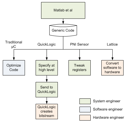
Figure 2. Sensor hub design flows and who does them.
Note that doing FPGA design might have organizational implications – or it could entail contracting out a solution if the company doesn’t have in-house skills. And the QuickLogic approach might not scale well if they prove too popular and get overwhelmed with design work; they would need to have a Plan B ready in case they experience that good problem.
Before we close off our look (for now) at sensor hubs, there’s one more wildcard in the offing, as noted by the aforementioned Mr. Whyte: Android 4.4 has specific sensor hub requirements. While Android isn’t a “standard” per se, it might as well be. And when things reach the level of standard, then you lose flexibility. And when you lose flexibility, then software becomes less valuable.
So, in the next installment in this series of articles, we’ll look at Android 4.4’s sensor-hub requirements. They could result in more hardware sensor hubs. Or so it sounds…
*On further reflection, concurrency could be useful to simplify synchronization. Sensor data has to be time-stamped, so that samples from different sensors can be correlated, due to the fact that sensors are polled serially. That could theoretically be addressed by parallel polling, but frequencies so far aren’t high enough to merit that level of complexity.
More info:


We’ve looked at the implications of different sensor hub architectures for performance and design. What other issues and implications do you see?
So Bryon-in your opinion which of the 4 sensor solutions described in your article will most likely be favored by OEM/integrators?
Oh, so now you’re going to put me on the spot, eh? After all the effort I went through to remain neutral? 🙂
Honestly, and sorry if this seems wishy-washy, but I don’t think there’s one right solution for everyone. For basic stuff, something like Sentral removes a lot of the need to know anything about the internals. Which is great if you don’t want more control.
Phone OEMs, by contrast, desperately want to differentiate their phones, so they’re going to want to dig in and control their own algorithms far more than, say, some wearables company.
I’m concerned that hardware design makes it harder for systems guys to specify and get the fusion features they want, but there are some open questions there: the full potential of FPGAs in that space hasn’t been proven yet, so if the results are compelling enough, people will go through the extra work. I’m actually expecting to hear more from them shortly, and I will share what I learn.
Finally, in the last week, there has been a slew of “platform” or “reference design” announcements. These go further than just the sensor hub; they’re full-up subsystems (or all of the required ingredients). The game is clearly becoming one of “who can get the best performance for the least work.” That favors canned or software-based solutions – especially since I don’t believe that, so far, any of these platforms features an FPGA. But I have to study them further, and I’ll be doing a writeup on them.
Did I dance enough to avoid a direct answer? (Seriously, I wish there were one simple answer)