

A dozen or so years ago, chipmakers ran into an issue. Features on chips were getting too small to print, and fundamental changes in how they were being printed (ahem: EUV) were long delayed.
The problem is that you’re not supposed to be able to get good feature resolution for feature sizes too far below the wavelength of light used to expose the wafer. The smaller you go, the worse things get. And these days, we’re small.
The saving grace came in two forms. You might think of one as pre-distortion: if the end of a line is going to get shortened and rounded, then you use a mask that has the line slightly lengthened and fattened at the end so that it winds up closer to what you intended. “Dogbone” ends are the most familiar such tweak. The other is more subtle: it consists of quaintly-named “decorations” (or boringly-named “assist features”). These are little bits and bobs on the mask that won’t actually appear printed on the wafer, but they will affect how neighboring features are printed.
And so we now have optical proximity correction (OPC) or reticle enhancement technology (RET) that lets us coerce and cajole 193-nm light into printing fine features well enough to do the job. Of course, someone has to do the work of figuring out what enhancements are needed to give the best result. That was once done by rules, but things have gotten too complicated for that. So it’s more likely to require simulation or, more recently, calculating what is essentially an inverse transform: take the desired pattern and back into what the mask has to look like. In particular, the latter, known as inverse lithography technology (ILT), gives an ideal result that must then be put onto a mask. And that’s getting harder.
Masks have benefited from a couple of advantages over wafers. Because only a few masks are made and quality is critical, throughput is less important for masks than it is for wafers (note: “less important,” not “unimportant”). So they’re made using an e-beam writer. The benefit here is that, unlike the wafer, you’re not exposing the whole thing at once: you’re exposing only a single dot or feature at a time. Each of those is a “shot,” and a mask is made by, well, shooting lots of shots. The more shots, the longer it takes. The electrons delivered during a shot constitute the “dose.“
The other advantage masks have had is simpler but disappearing: masks features are normally four times larger than the wafer features they will create; the shrink happens optically. That means that they’ve been behind on feature size and have had fewer issues. But that’s changing. Being four times larger than ridiculously miniscule can still be ridiculously small.
In particular, you can no longer assume that a dose is a dose is a dose. You now have to deal with “dose margin,” a rough agglomeration of all the different kinds of variation that might occur as you’re shooting the mask, all of which mean that a given shot might involve more or fewer electrons. That means the specific shape or size of a shot is no longer certain.
So now it’s no longer enough to compensate for wafer exposure weirdness by making the mask look all bizarre; now we have to compensate for mask exposure weirdness too. It’s as if we now need to pre-distort the pre-distortion. Compensation is pushing back one level. D2S CEO Aki Fujimura refers to it as “double simulation”: you have to simulate mask-to-wafer and e-beam-to-mask interactions.
The effect on mask-writing time is compounded by the otherworldly patterns that ILT might predict are required to print on the wafer. Mask-making techniques generally involve turning shapes into a series of rectangles (even though, at fine geometries, a shot is closer to a circle than a rectangle). The more oddball the pattern, and the more curvy it is (or “curvilinear”), the more rectangles it takes to approximate that shape with acceptable jaggedness. (This process of turning curved shapes into a series of rectangles is referred to as “Manhattenization,” proving that it’s possible to create a verb out of anything and then back-form a noun out of that. I.e., it’s easy to nounify verbified nouns.)
This is where a seemingly trivial consideration comes into play. When “fracturing” the pattern into rectangles, you can often get fewer rectangles if you allow the rectangles to overlap. Problem is, this is something that conventional fracturing technology doesn’t allow. So in the figure below, the shape on the left requires 7 rectangles if they’re not allowed to overlap (middle image). If they can overlap, you cut the number down to 4* (right image).
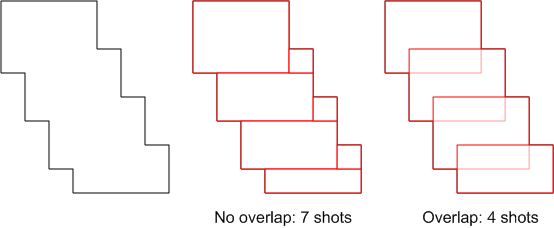
Figure 1. Overlapping rectangles results in fewer rectangles.
Where all of this is leading to is an announcement by D2S about their new TrueMask MDP (mask data preparation) tool. They claim to reduce mask prep time by 20-30% for conventional shapes and Manhattenized ILT shapes and by 30% for “ideal” – that is, non-Manhattenized – ILT features.
One of the main features they tout is the ability to handle overlapping shots. As we’ve seen, that can mean fewer shots – and therefore faster mask writing. By combining such overlap with variable-shaped beams and a customized dose for each shot, they claim not only to speed things up, but also to improve the quality of the mask – specifically the dose margin – and therefore the quality of the wafers that will be produced using that mask.
In addition, this is also apparently the first model-based MDP that can handle an entire chip at once.
So, naturally, this simulation is going to be computationally intensive. Which is why they are also providing a purpose-built acceleration platform, called the D2S Computational Design Platform, that exploits the parallelism in the problem. The entire chip is gridded, and each resulting square is sent to a different processor to be worked on. Combining conventional CPUs and graphics processors for 400 TFLOPS, they claim to be able to process 80-300 billion shots per day without relying on speed-up approaches like hierarchy and pattern matching. That more or less amounts to one chip per day.
So the step function in work necessary to figure out what the mask should look like, which was encountered more than a decade ago, has now arrived to plague the determination of how to shoot the mask so that it will have an accurate rendition of the strange-looking shapes that will result in the wafer being exposed with a “simple” pattern.
That’s a lot of work required to cheat the laws of physics. Now… if EUV would just hurry up, we wouldn’t need any of this.**
*The rectangle savings isn’t always this good; I was playing with a more arbitrary shape and found that, in that case, the number of overlapping rectangles was always the same as the number of non-overlapping ones… a result that I take to be only empirical at this point… a proof of equivalence, if it exists, is left to the reader.
**Famous last words.
More info: D2S


Have you had issues making masks quickly and with high enough quality at 28 and 20 nm? What have you done about it?