

There are certain companies that seem to make their living with what some marketers call a “fast follower” strategy. The principle is sound and simple. You watch the leading bleeding-edge companies in your market segment. You take note of which of their new products gain market traction, and you create a useful, usable substitute for those products for a significantly lower price.
Just about every industry has companies that could be characterized as “fast followers.” In EDA, one might argue that Aldec is such a company. Aldec has long made their way by offering a solid, useful HDL simulation platform for significantly less money than most mainstream vendors. Aldec’s simulators have gained a reputation for excellent reliability and usability, and they have particularly earned a strong following in the high-reliability and military/aerospace segments.
As a market becomes commoditized, however, the fast-following strategy begins to break down. When the leading vendors can no longer charge a premium for their product, they have to reduce their prices to more sustainable levels. That, in turn, puts even more downward price pressure on the fast followers. In software, this is often the time that open-source or free options also materialize, squeezing the fast followers from the bottom as well as the top.
In Aldec’s case, they’ve avoided the fast-follower trap by growing their product offering into the vast expanse of verification technologies. With the fast pace of Moore’s Law, verification engineers are constantly under pressure to become more efficient and more effective. That means more complex tools and more advanced methodologies – which keeps the premiums in the pricing for EDA companies.
Aldec’s latest foray into the bigger world of verification takes them into hardware – FPGA-based prototyping boards, to be specific – and that move may have quietly slipped them from “fast follower” into “inadvertent leader.”
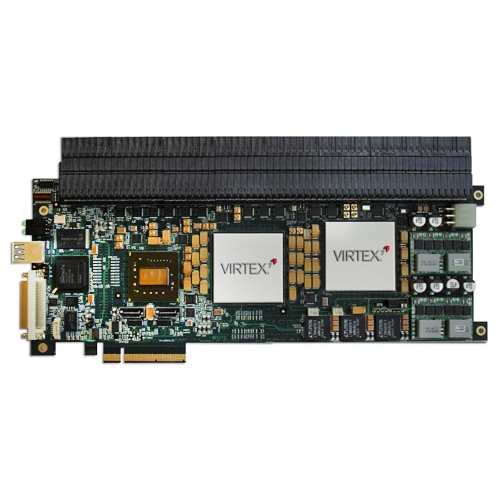
Aldec has just announced their new “HES-7 ASIC Prototyping” system. This announcement puts them into a market where they have not been seen in the past. By introducing an FPGA prototyping board, Aldec put themselves up against vendors like Dini and Synopsys (Hardi/HAPS), as well as emulation solutions like Mentor, Cadence, and Eve. In the tradition and style of fast following, however, Aldec’s solution is modest in some ways. With only 2 FPGAs on a comparatively tiny board, it looks like a much smaller solution than most of the mainstream offerings. However, those 2 FPGAs are Xilinx’s newest, biggest, Virtex-7 V2000T devices, built on the completely new 2.5D interposer-based packaging technology. Aldec conservatively estimates the ASIC gate capacity of this board at 24 million ASIC gates.
This is where it starts to get interesting.
As far as we know, Aldec is the first company to get to market with a prototyping board based on the new “world’s largest” FPGA. In the general FPGA space, the V2000T is regarded more as a grand experiment than a practical device – with a price tag that makes it economically unsuitable for most applications. The prime exception to that “most” is ASIC prototyping, where the enormous LUT resources on a single device give a dramatic boost to the size of design that can be prototyped without complex multi-FPGA partitioning. With just two V2000T devices, this board has as much capacity as other boards containing many more FPGAs. Fewer (and larger) FPGAs means less partitioning is required to get your design up and running, and that relieves one of the biggest headaches in FPGA-based prototyping.
Partitioning a large design across several FPGAs is harder than it sounds. You need to cut your RTL up into bites that will fit inside each of the target FPGAs, and then you need to connect those parts of the design via available IOs on your FPGAs. In many cases, it’s difficult to get the size of the partitions right so they each fit into an FPGA and to also keep the required number of connections between FPGAs below the number of available IOs. Often, the design hierarchy required to accomplish this is nothing like the natural design hierarchy you want for your finished ASIC design. Once that issue is solved, you also have to contend with timing issues. If critical timing paths end up crossing the boundaries between FPGAs, you’ll have a big ‘ol mess that will require optimizing, fixing, and re-partitioning. Finally, the more stuff you have to do to your design to get it to work on the FPGA prototype, the farther you may be deviating from your main design, and that can spell trouble if you end up prototyping something that’s significantly different from what you’re eventually actually building.
There are, of course, automatic partitioning tools that can (attempt to) handle this for you, but those are hit-and-miss. Typically they partition the design after synthesis, so you don’t have as much of a solid mapping from the design you created to what you’re seeing on your prototyping board. Often, users report that the automatic tools are difficult to control, and that they give wildly varying results depending on the topology of your particular design.
Of course, the best way to avoid partitioning headaches is to avoid partitioning in the first place. With Aldec’s boards being based on enormous new FPGAs, the most partitioning you’re likely to need is across 2 devices. That is a much more manageable problem than trying to cut up a bunch of RTL across five or six FPGAs. Less obvious is the benefits that this brings when you go to actually use your prototype for debugging. When the design is not sliced and diced into a bunch of seemingly arbitrary partitions, it is much easier to locate and isolate trouble spots.
The new Aldec HES-7 ASIC Prototyping system is priced as if it came from a fast follower. The system starts at under $20K, which, depending on which rumors you believe, may not be much more than the price of early V2000T devices. Aldec will be offering a range of configurations (four boards plus a backplane) that can easily scale to fit your needs. The smallest is rated at about 4 million ASIC gates and boasts a single XCVX690T FPGA. Up from that, rated at 8 million gates, is a board with two of those. Moving up from there, we go to the big V2000T device for a 12-million gate capacity, and finally to the biggest board with two V2000Ts for a 24-million gate total.
If the 24-million gate single board doesn’t cut it, the HES-7 backplane can handle four of the largest boards, giving you 96 million ASIC gates of capacity which, best of all, is spread across only 8 FPGAs. That’s a feat that could not be accomplished with any existing prototyping technology.
Aldec wisely chose non-proprietary high-speed 25 Gbps connectors for the expansion, backplane, and daughterboard interface. Their board is simply and efficiently designed, with 322 high-speed inter-FPGA connections, 5 global clock inputs, and 89 special-purpose global lines connected to all FPGAs. Up to 16 GB of DDR3 RAM is supported with SO-DIMM sockets, which gives up to 64GB with 4 boards on the backplane. There is also 8GB of flash memory attached to FPGA0 and a micro SD card socket for stand-alone configuration. The board is large form factor PCI with PCI-Express finger connectors – allowing inside PC operation, and there is also a PCI-Express cable connector for outside PC operation. Rounding out the connectivity are things you’d expect like USB 2.0/3.0, JTAG, and 2 SATA connectors.
As interesting as Aldec’s initial entry into the prototyping board derby may be, the real intrigue will be seeing what software tools are eventually integrated with the board. With Aldec’s capabilities and experience in verification tools, one can easily envision a robust set of tools and capabilities smoothly integrated with this affordable, high-performance, scalable prototyping platform. We’ll be excited to see if that happens.


Aldec has ventured into the FPGA-based prototyping space. What do you think?
I’ve dealt with HES-1 a decade ago. At that time Aldec was a close partner of Xilinx, and had installed a newest and biggest FPGA chip XCV800 in its board. It was very simple board from present point of view. But it provided the modeling speedup up to 100 times. I has proven it in the project of a custom GPS receiver. Without a HES board I had to model a test of a satelite signal receiving for ca. a week.
Now we see a turn around – Aldec introduced the HES-board with the high-end chip once again.
Apropose, the prise of HES-1 was even higher than one of HES-7.