


A big chunk of the vast, imagined IoT (Internet of Things) includes the industrial IoT (IIoT), which is responsible for controlling and monitoring energy-consuming processes based on large motors, pumps, fans, generators, heavy-duty actuators, heaters, and other high-power equipment. Such IIoT applications aren’t as concerned with low-power design compared to the medical and consumer side of the IoT—wearables and the like. Medical and consumer IoT designs are more sensitive to high-volume unit costs and low-power considerations, which makes them good targets for ASIC implementations.
The semiconductor foundries have developed low-power and low-leakage processes including FDSOI variants that suit these low-power IoT applications, as long as the applications demand the sort of high manufacturing volumes that would support a full-on ASIC development project. Microprocessor IP vendors have developed low-power processor cores that can be used in such applications. The modular RISC-V and Arm Cortex-M series processor cores are but two examples. But the ever-present SRAM IP has been left out of this equation, or so claims sureCore CEO Paul Wells.
“SRAM IP has not changed in 20 years,” Wells told me at the recent DAC held in San Francisco last June. There’s a simple reason for that, he explained. For the last 20 years, simply waiting for the next semiconductor process node to come on line would automatically give SoC designers faster memory that operated at lower power levels. Because there were plenty of other fires to extinguish and mountains to climb, on-chip SRAM design stagnated.
That was before Dennard Scaling and Moore’s Law went to their graves. (If you read EEJournal regularly, the deaths of these two industry stalwarts should not come as a surprise. For example, see “Fifty (or Sixty) Years of Processor Development…for This? ‘Dennard Scaling and Moore’s Law are dead, Now what?’ – a 4-act play by Dr. David Patterson” and my more recent blog titled “Monty Python, Dead Parrots, Moore’s Law, and the ITRS.”)
The IoT has the potential to require stratospheric, mobile-phone production volumes that make electronics vendors’ mouths water. But without the relatively large lithium batteries that come along with mobile phones and certainly without the ready juice fix of a daily (or nightly) recharge, these IoT designs need to sip power. Today, everything IoT seemingly needs to run on small, coin-cell batteries or locally harvested power and needs to run essentially forever. That’s a tall order.
The coincident deaths of Moore’s Law and Dennard Scaling along with a sudden strong interest in millions of low-power “things” that connect to the Internet have opened a market window for new, on-chip memory IP, which prompted sureCore to develop 6T SRAM blocks that could operate at very low voltage, reducing dynamic power levels by as much as 80%. The resulting SRAM design for TSMC’s 40 ULV process technology can operate at supply voltages as low as 0.6V across process corners and over the full industrial temperature range of -40° to 125°C.
Achieving that feat required the sureCore designers to toss out a lot of excess design margin, which in turn required a significant amount of “high-sigma” statistical simulation and analysis to ensure that there was still sufficient margin for the SRAM to operate over process variations, without process modifications, and even down to 0.6V. Monte Carlo simulation and extensive physical verification including IR drop, electromagnetic interference, and crosstalk checks replaced typical, fast-and-loose, she’ll-be-right-mate engineering margins. The result is sureCore’s EverOn low-power SRAM IP core.
Figure 1 below shows a graph that plots energy consumption versus supply voltage for the EverOn SRAM core built in TSMC’s 40 ULV process technology versus factory SRAM IP. The graph’s taken from sureCore’s EverOn data sheet:
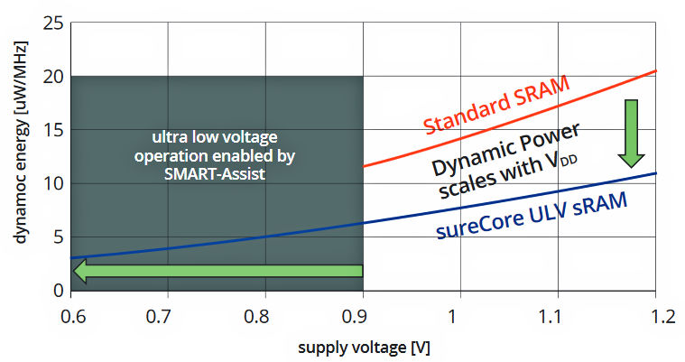
Figure 1: The sureCore EverOn SRAM consumes less power at the same supply voltage and operates at much lower power at low supply voltages compared to foundry SRAM.
Three key things to note from this graph:
- The sureCore EverOn SRAM always consumes significantly less power than standard foundry SRAM at any supply voltage.
- The sureCore SRAM continues to operate down to 0.6V, much lower than the characterization curve for foundry SRAM, which stops at 0.9V.
- In the most extreme comparison, the EverOn SRAM core operating at 0.6V consumes less than 20% of the energy per MHz compared to the foundry SRAM core operating at 1.2V.
In addition, sureCore’s EverOn SRAM design divides each SRAM core into four independently controlled banks. Each EverOn SRAM bank can be active, asleep (with data retained), or off, as shown in Figure 2 below:
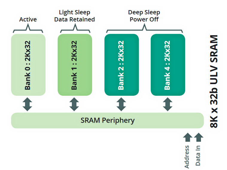
Figure 2: All EverOn SRAMs are divided into four independent memory banks and the operational/power state of each bank is under software control, which can result in even lower power operation.
The EverOn core’s control circuitry allows software to control the state of each of the four banks and the SRAM periphery circuity, making even lower power operation under active software management possible. You power up only the RAM you need, when you need it.
So what’s new here? Hasn’t near-threshold ASIC logic been around for a while? Yes, said Wells, but foundries’ ASIC SRAM bit-cell designs have not followed. Because SRAM blocks are stepped and repeated and because they consume relatively large amounts of on-chip area, standard-cell SRAM IP is designed for optimal packing density, to save silicon area and not to save power. Remember, saving SRAM power was once a simple result of Moore’s Law, Dennard Scaling, and process-node migration, so SRAM IP didn’t get redesigned when there were so many other, more important things to do.
With Moore’s Law and Dennard Scaling dead and on-chip process variability on the rise in the land of nanometer process geometries, the possibility of “weak” bit cells in an SRAM block increases. This weakness materializes operationally in the form of multiple problems that produce random read and write errors when the SRAM block operates at near-threshold supply voltages. That’s why the factory SRAM curve in Figure 1 above stops at 0.9V.
Engineers know you rarely get something for nothing, and that’s the case here too. First, EverOn SRAM blocks are 5-to-10% larger than big standard foundry SRAM blocks. Second, there’s about a 10% performance loss if you lower the supply voltage all the way down to 0.6V. However, you get full speed if you wind the supply voltage up to 1.2V.
Now the EverOn SRAM’s area penalty might seem like it’s an issue, but there are a couple of factors to consider. First, sureCore’s EverOn SRAMs are intended for less memory-intensive applications (meaning they’re NOT intended to store images, audio, video, or large blocks of code). These are relatively small memories that max out at 8K by 72 bits or 16K by 36 bits. That’s 576 Kbits, if you do the math. These EverOn SRAMs are designed to hold small blocks of code and tiny data sets—which are more appropriate for wearable IoT devices or smart dust sensors.
The EverOn memories must be small to effectively manage process variation, and sureCore has run test chips in TSMC’s 40 ULV process to prove the design. Standard 125°C, 1000-hour, HTOL (High Temperature Operating Life) tests on these chips surfaced no PVT failures in the SRAM design. In other words, there’s still sufficient design margin to achieve reliable operation as proven by all that time at Monte Carlo.
Second, the conventional approach to building low-power, low-voltage bit cells for SRAM IP is to use a 10T cell design, which is a 67% increase in area over a 6T bit cell. By comparison, the EverOn SRAM core’s 10% area penalty really doesn’t seem like all that much.
That left one potential fly in the ointment for me to investigate. I asked Wells about the adoption of TSMC’s 40 ULV process technology, and he admitted that the uptake at that process node wasn’t as great as expected. He then added, “That’s why sureCore has migrated the EverOn design to TSMC’s 28 HPC+ process technology.” Now 28nm process technology is the current sweet spot for ASIC density/cost and it’s destined to stay that way for quite a while. FinFET technology and EUV lithography increase the cost of ASIC design and manufacturing, so 28nm processes like TSMC’s 28 HPC+ are going to be in the Goldilocks zone for IoT devices for the foreseeable future.


