

Sunnyvale, CA, December 10, 2015 – Zeno Semiconductor today announced its novel 1-transistor Bi-SRAM (bi-stable, intrinsic bipolar) memory technology at the IEDM Conference. Zeno’s 1-transistor Bi-SRAM uses a single transistor as the memory bitcell and is therefore 5x smaller than conventional SRAMs which use 6-transistor bitcells (6T-SRAM). When implemented in 28nm, the high density Zeno, which is 37% smaller than Samsung’s recently-announced world’s-smallest 6T-SRAM bitcell of 0.040 ?m2 implemented in the company’s 10nm process technology, and 5xBi-SRAM cell size is 0.025 ?m2 smaller than the conventional 0.127 ?m2 SRAM bitcell at the 28nm node. The IEDM paper is titled “A Novel Bi-Stable 1-Transistor SRAM for High Density Embedded Applications” and is co-authored by researchers from Zeno, Marvell Semiconductor, and Stanford University.
Unlike all other single-transistor bitcell memories that operate dynamically by storing charge on a capacitor that leaks and requires refreshing, Zeno Bi-SRAM bitcell is truly static – the memory will retain state indefinitely without any sort of refresh and is therefore an SRAM. The Zeno technology achieves this by utilizing the intrinsic vertical bipolar transistor that is present in all conventional CMOS and FinFET processes. In addition, because of the single transistor bitcell and smaller overall array size, Bi-SRAM will consume lower power. The company demonstrated these results in silicon test chips implemented at the 28nm node, and has analyses showing similar benefits in FinFET technologies.
Furthermore, in contrast to other next-generation memory technologies, Zeno’s Bi-SRAM technology is manufacturable on conventional CMOS and FinFET processes without any new materials or equipment. The technology uses a buried n-well implant under the memory array – which means any existing libraries, circuits, and IP will be unchanged and have exactly the same characteristics.
TARGET MARKETS INCLUDE INTERNET OF THINGS (IOT), MOBILE, CONSUMER, AND HPC, NETWORKING
In addition to its flagship 1-transistor (1T) Bi-SRAM, Zeno also introduced its 2-transistor (2T) Bi-SRAM technology. Although larger than its 1-transistor sibling, the 2T bitcell is still 3x smaller than a conventional SRAM bitcell, and can match or exceed the performance of the fastest embedded memories.
“We have created two versions of the technology to target different market requirements,” said Dr. Yuniarto Widjaja, Founder and CEO of Zeno Semiconductor. “The 1T Bi-SRAM is targeted at cost-sensitive, low-power applications such as IoT, while the 2T Bi-SRAM technology is targeted at high-performance applications such as networking and high-performance computing (HPC). What is interesting is the relative benefits of the technologies carry over from one process generation to another – that is, the relative area and power improvements you see at 28nm will be seen in FinFET technologies as well as older nodes.”
“Of course, like any SRAM technology, we can make trade-offs among area, speed, and power to create a specific operating point,” continued Dr. Widjaja. “The following table helps to highlight the relative benefits compared to well-known baseline technologies. This table was generated as a 28nm comparison for the cell and 1Mb macro, but we believe the same general benefits will apply at newer and older process nodes.”
TABLE COMPARING ZENO TECHNOLOGY TO CONVENTIONAL SRAM SOLUTIONS
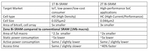
“Zeno Bi-SRAM allows for reduction of on chip SRAM area by over a factor of two, giving designers the opportunity to more than double the SRAM density or significantly reduce the die size”, said Stefan K. Lai, a former VP of Intel’s Technology and Manufacturing Group and a member of Zeno’s Technical Advisory Board. “This is accomplished with simple addition of a few standard process steps and no change in design rule. This is truly a breakthrough in embedded memory technology.”
BUSINESS MODEL AND AVAILABILITY
Zeno’s business model is to license the 1T Bi-SRAM and 2T Bi-SRAM technologies and IP to semiconductor and foundries. Licensees can implement their own memory macros, or they can contract with Zeno to do so. The technology is available for customer engagement today; please contact Zeno for more details.
ABOUT ZENO SEMICONDUCTOR
Zeno Semiconductor, Inc. (www.zenosemi.com) develops and licenses novel memory and logic technologies which provide innovative paths to scaling semiconductor devices. The memory and logic technologies are manufacturable on mainstream CMOS and FinFET fabrication processes with no new materials or equipment, and with no changes to any of the existing libraries and IP. Zeno currently has been awarded more than 50 patents. Contact Zeno at contact@zenosemi.com.


