

Some months ago, Applied Materials (AMAT) announced an atomic-layer product. Then Lam had a couple of announcements. And finally, more recently, ALD NanoSolutions had something to say. It’s like, just when you’re ready to write something up, there’s yet something new.
So… on the assumption that we’ve got all the atomic-layer news spread out on the desk and that there are no other news stories lurking, how ‘bout we go through these to find out what’s happening at the atomic level.
The Opposite of ALD
We all know what ALD is, right? No? OK, just to get us all baselined, it’s atomic-layer deposition. And it’s a pretty cool trick. It’s good for when you need only one atomic layer of some… substance. OK, realistically, so far, we don’t need just one layer so much, but when you’re trying to build a really thin, precisely deep film of some sort, this does the trick.
It’s a two-step process: first admit a precursor chemical that binds to the surface – meaning that, when the surface is covered, there’s no place else for extra to stick. So you get exactly one layer, and it’s self-limiting. Then you admit another chemical that reacts with the first layer and creates the film you want. Since there’s only one layer of the first precursor, then you end up with only one layer of the product. Again, self-limiting. Rinse and repeat until you get your desired thickness.
So that’s deposition; what would the opposite of that be? Etch, of course. This would be ALE (E being the natural follow-on to D): atomic-layer etch. We’ve had wet etch and dry (plasma) etch to work with for years; why do we need yet another approach? AMAT gives a couple of reasons.
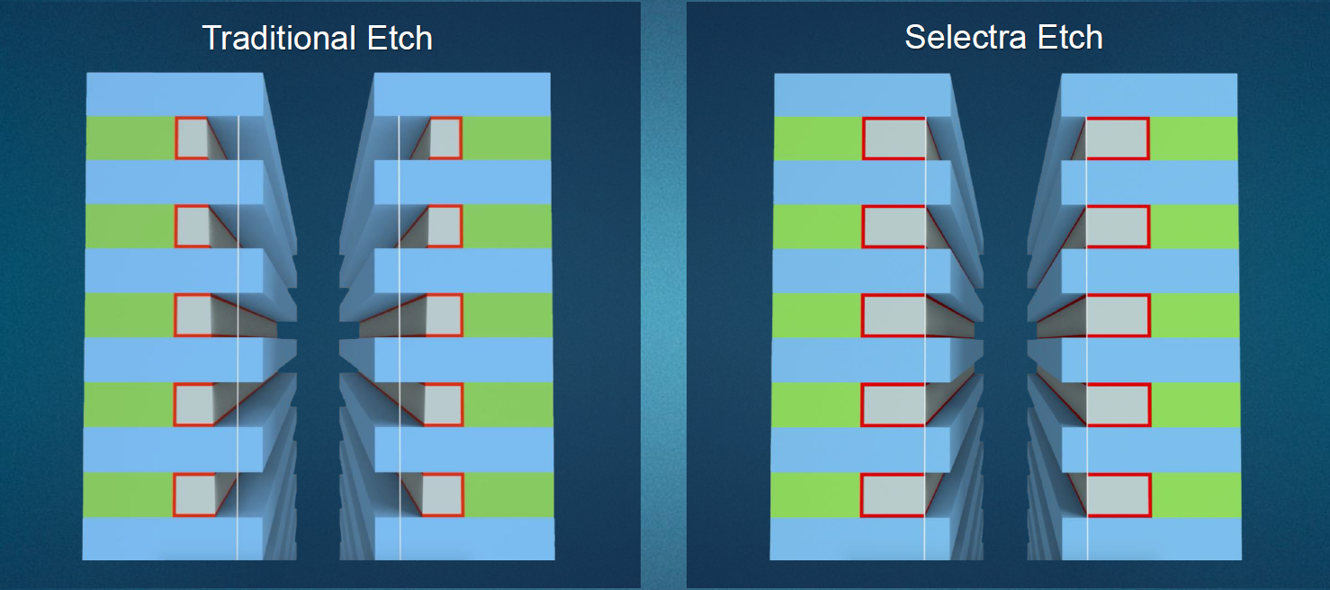
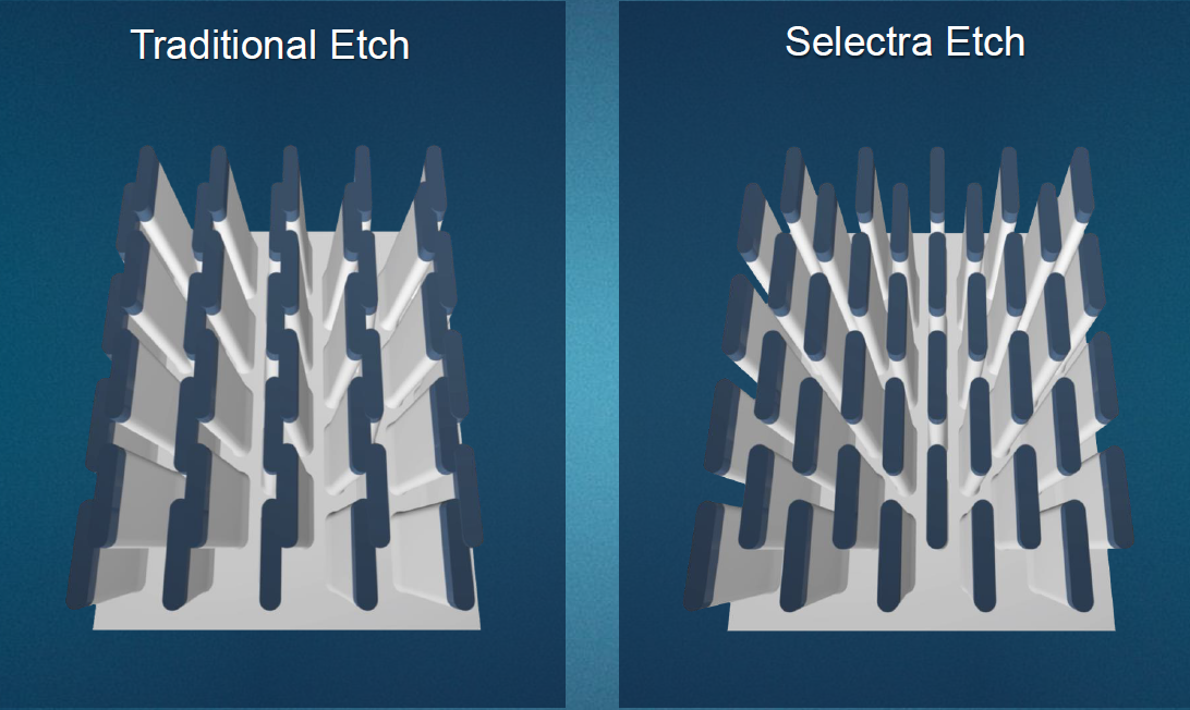
Wet etch starts with hazardous chemicals, so if we can get away without it, so much the better. But from a performance standpoint, there are two main challenges. The first is the impact of high-aspect-ratio (HAR) features: tall pillars and such. They tend to collapse with wet etch. The second issue is that, if you have narrow spaces, the etchant may not penetrate all the way in, giving uneven results.
On the dry side, much of the etching effect comes from brute-force bombardment with ions. That is somewhat selective, but not nearly as selective as we’d like. The other issue is that most etching happens in the direction of the bombardment – vertical. Lateral etching doesn’t work so well.
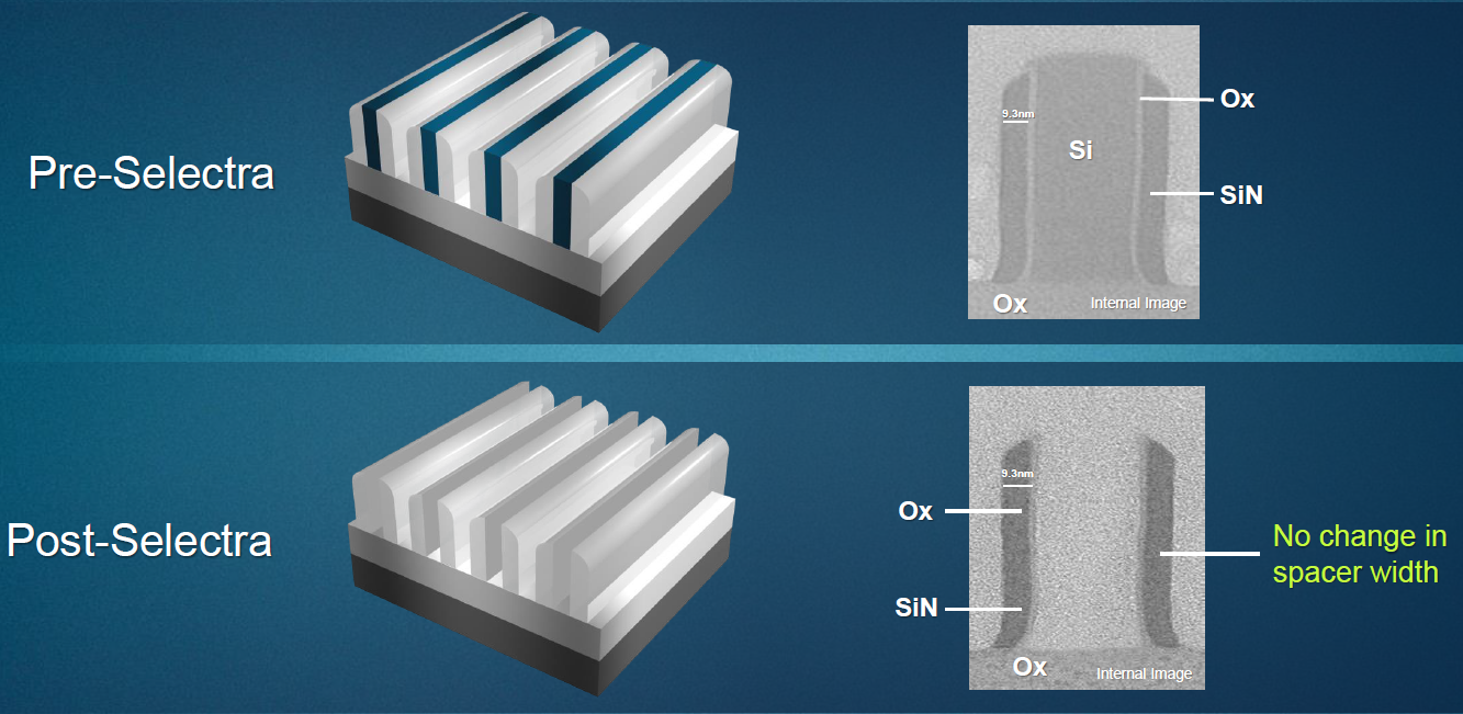
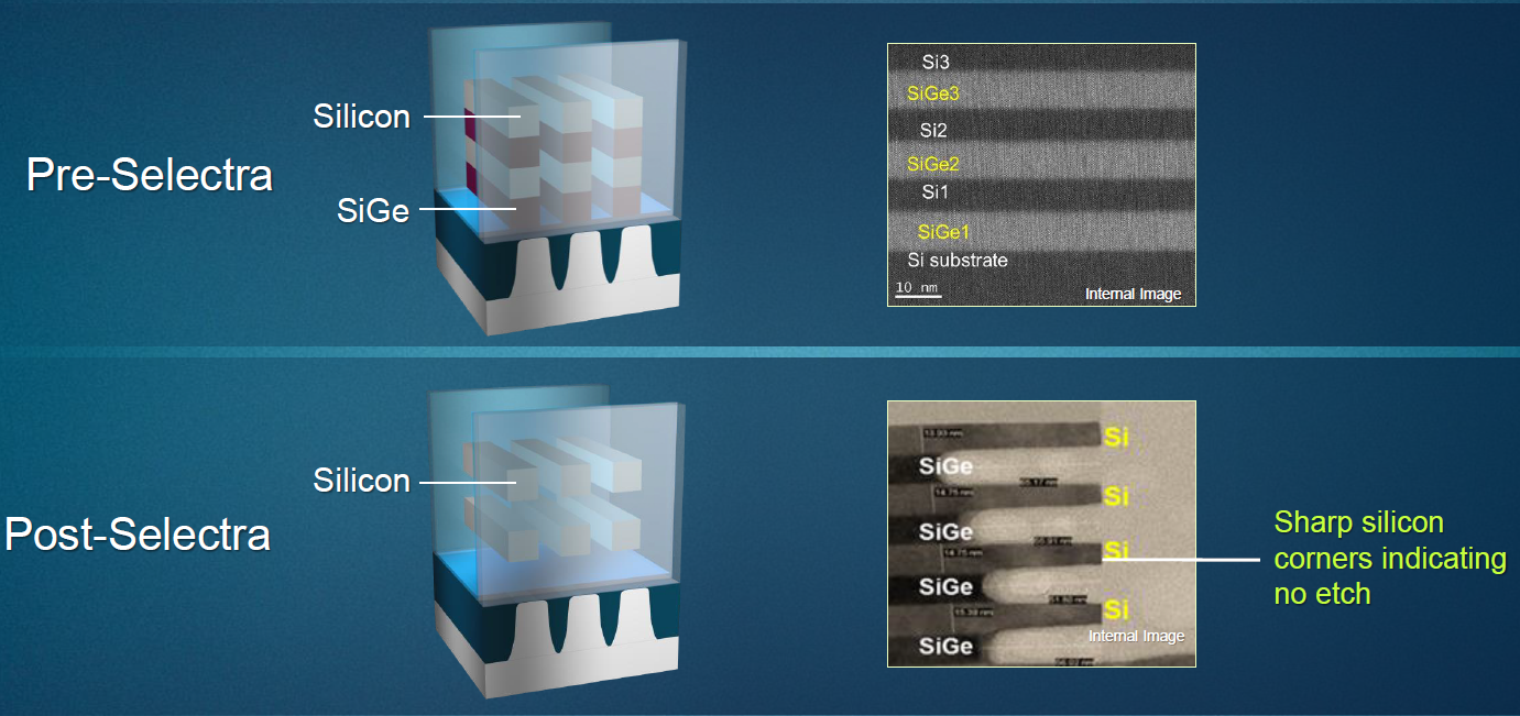
So AMAT’s Selectra system addresses these past issues. You might wonder, if we’ve done just fine so far, why is this all of a sudden a problem? Well, nothing is “all of a sudden,” but we’re now crying “Uncle” based on a few specific scenarios – at least. Selectivity is key for high-fidelity formation of multi-patterning guides; it’s also important for forming gate-all-around (GAA) structures – useful for post-FinFET transistors. Precise lateral etching is really useful for forming complex 3D NAND pillars. And the HAR thing is needed for future DRAM capacitor formation.
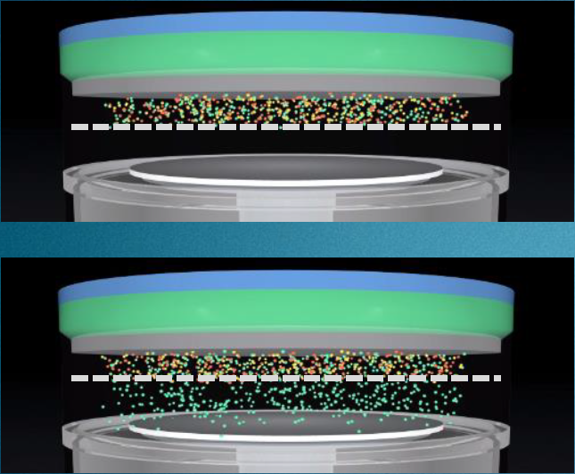
How does AMAT do this? It actually uses well-known plasma chemistry, which creates both ions and radicals. The difference is that they filter the ions that normally do the work and, instead, permit only the radicals to go through, ensuring a chemical-only etch. Choosing the chemistry then gives excellent selectivity.
(Image courtesy Applied Materials)
If you’re like me, you might wonder how it is that the radicals can get all the way into the deep interstices – don’t they have to displace air or whatever’s in there? If so, you’d be reminded, as I was, that this happens in a vacuum, so there’s nothing to displace. Quite the opposite: nature would welcome something to assuage its abhorrence, so the radicals can go absolutely anywhere they want. But they etch only when meeting the correct target substance.
They showed conceptual images and a few photo images illustrating the concepts. So we have:
- For multi-patterning:
(Click to enlarge. Image courtesy Applied Materials)
- For gate-all-around:
(Click to enlarge. Image courtesy Applied Materials)
- For 3D-NAND:
(Click to enlarge. Image courtesy Applied Materials)
- And for HAR DRAM structures:
(Click to enlarge. Image courtesy Applied Materials)
On the Lam
Meanwhile, Lam Research has also announced ALE. And their approach is completely different – and much more like standard ALD. They use a two-step process that starts with a precursor that binds to the top surface; they then bombard with something else to knock off that first layer – and nothing below it. For silicon, they use chlorine gas as the precursor, with argon ions then used for the actual removal.
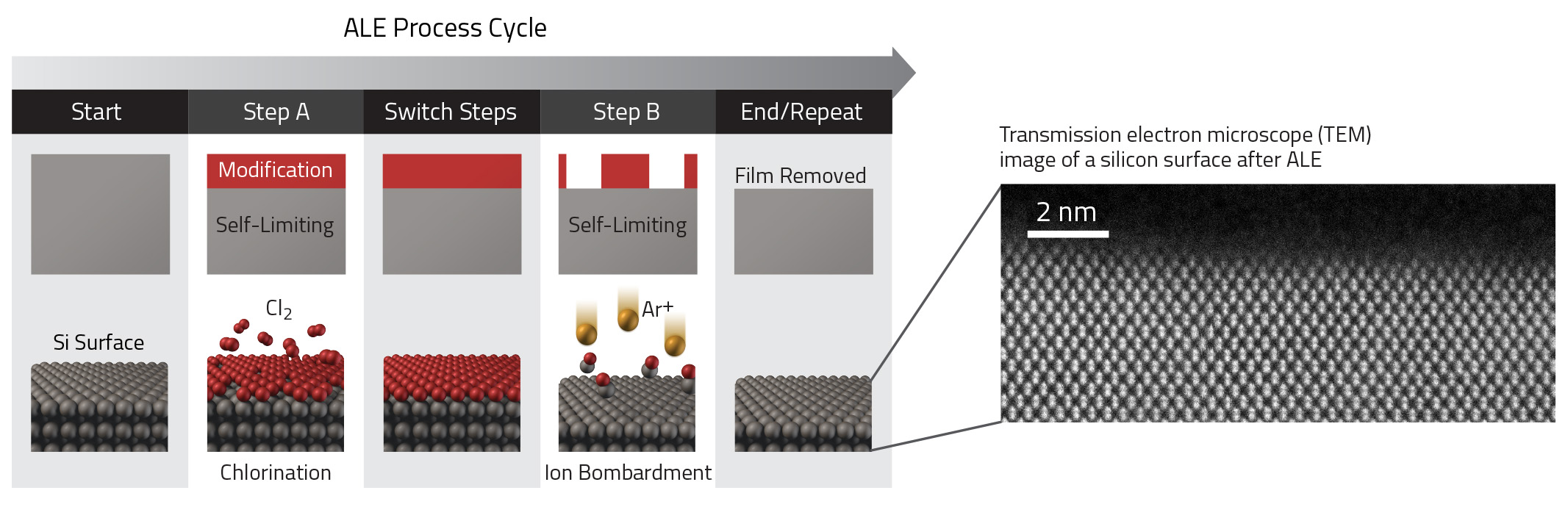
(Click to enlarge. Image courtesy Lam Research)
The downside to this approach – as compared to AMAT’s – is that you have the two-step pulsed process, which is a bit fussier. One benefit is that it’s self-limiting: you do only one layer at a time, giving atomic-level control. The AMAT approach doesn’t technically go layer by layer, and the appropriate stop time isn’t built into the process: it’s simply a matter of how long the reaction runs. It’s open-loop, so characterization of the reaction times is critical to precision.
Separately from the ALE announcement, Lam also announced a new ALD development. The headline focused on the reduction in residual fluorine, which sounds like a nuance, but there’s more to the story than this. To get it all in proper perspective, we need to go back a generation or two.
The problem we’re addressing here is the filling of holes like contacts and vias with tungsten. Two things have to happen: first a nucleation layer, then a bulk fill. The nucleation layer gives the bulk fill a toe-hold, if you will.
Chemical-vapor deposition (CVD) was once the standard go-to process for both of these steps, but, at some point, ALD took over the nucleation layer, while CVD continued its role for bulk fill because it’s just easier and faster than the fussier (but more precise) ALD process.
So it seems to me like the big story here is that Lam has leveraged ALD for bulk fill as well – CVD has left the building. One of the benefits of using ALD is that it leaves less residual fluorine than CVD, which improves metal integrity and removes stresses. Which motivates the original fluorine focus of their story.
ALD for Particles, Polymers
Finally, and most recently, I received an announcement about ALD NanoSolutions having had a “banner year.” Financial results aren’t something I typically focus on, but here we had what seemed like yet another ALD player that I wasn’t familiar with. So I thought I’d check them out too.
Turns out they play a very different game from the one we’ve been looking at. They don’t do ALD for semiconductors; they focus on nanoparticles and polymers.
Let’s start with the particle thing. One of the big applications of this is for use in lithium batteries. You know, the kind that you can no longer bring onto a plane if it has the wrong brand on it. One of the things they do is to coat lithium ion particles so that the ions can’t assemble on a street corner, scaring pedestrians, clumping, and forming a conductive mass, which would get them, well, put on the no-fly list. They also coat the battery anode. All in the name of safety.
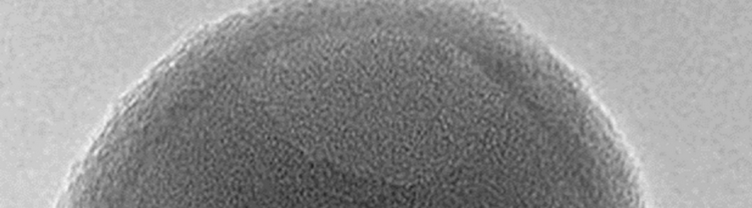
5-nm aluminum oxide layer on 40-nm silicon oxide particle
(Image courtesy ALD NanoSolutions)
The polymers apply more to thin-film electronics – of the sort that might go into your body as a medical sensor or other device. Or they might coat the tools, especially where this might provide better isolation between the tool and any drug that’s in contact with the tool. While there are a variety of chemistries that might apply to the polymer application, the only one they’ve been asked for so far is alumina.
So there you go. ALD and ALE from July through the present. You’re all up to date. (Which will assuredly earn me an email from someone else who had relevant news that I didn’t see…)
More info:
Applied Materials Producer Selectra
Lam Research Altus ALD (bottom of page)


What do you think of these atomic-layer processes?