

They call themselves Intel now.
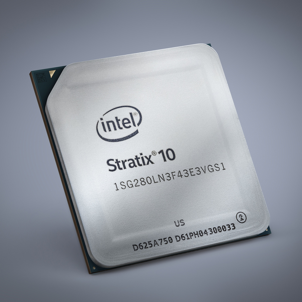
Sure, they still live in the Altera building and the technology is still unmistakably Altera’s, but the company has now turned the page, and the word “Intel” proudly silkscreened on the top deck of the company’s flagship Stratix 10 devices is a message to the world that things have now changed forever. For the past year or so, the sixteen billion dollar high-profile acquisition of Altera by Intel has been stewing in the pot – adding and removing ingredients, taste testing, and settling into the flavor profile that the newly re-formed organization wants to present to us.
It is now time for us to take our first taste.
The recent Intel Developer Forum (IDF) included a new segment – the SoC FPGA Developer Forum. At the keynote for that event, Intel CEO Brian Krzanich said, “Intel getting into the FPGA business in a big way was absolutely something that I drove personally in the company… I truly believe in the FPGA business, and this is something I am passionate about growing in the company.”
Of course, Intel must be pretty interested in the FPGA business, or they wouldn’t have spent the kind of cash they did to buy Altera. But many of us familiar with the FPGA industry have had ongoing concerns about Intel’s ability to understand and adapt to the unique characteristics of the FPGA business – that service and software are more important than silicon, that sockets are often won years before the associated revenue appears, and that products have a much longer life cycle in the field than Intel’s traditional offerings. Understanding of these key issues (or the lack thereof) could easily be make-or-break for Intel’s FPGA future.
Krzanich tackled the service aspect head-on in his keynote, explaining that Altera’s sales and support would remain independent but would have access to the full depth of Intel’s resources. He went farther telling customers that, “You should see nothing but an improvement, hopefully, in your service and support.”
Additionally, there are those (we are not among them) who have also worried that Intel would have a philosophical problem manufacturing chips that contain rival ARM processor cores (which is the case with all of Altera’s SoC FPGAs). “I can commit to you right here” Krzanich said, “that any product that’s built on an ARM core will continue to be built on an ARM core – as long as that core is what’s required to win the business and be the best performing product… There is no plan … to yank ARM out and stick IA in and make all you guys change your programming models.”
A few things are self-evident. First, Stratix 10 is late. If we were back in the old Xilinx vs Altera days, this would have been considered catastrophically late. When, exactly, will we see Intel Stratix 10? “I’m telling you right now,” Krzanich continued, “we are planning to ship by the end of this year.” When the dust settles, though, Xilinx will probably have delivered their UltraScale+ 16nm FinFET families more than a year before Intel/Altera puts the first production 14nm TriGate Stratix 10 devices out the door. In the old world, where each company’s stock price was tied perilously to each quarter’s news, and the biggest possible news was a lead or lag on the latest process node, a one-year deficit would have been a red flag of epic proportions.
But, these are not the old days. Intel’s fortunes do not rest solely on their ability to execute on their FPGA strategy (although all signs point to a future where FPGAs are of exponentially increasing importance to Intel’s bottom line). If Stratix 10 FPGAs and SoCs (and their associated design tools and IP) live up to their potential, there are vast green fields open for Intel to conquer – green fields that do not rely on being the first to market at the latest bleeding-edge process node. And, even though it’s good for bragging rights, the latest bleeding-edge node is not what will drive the programmable logic market in the years to come. Even today, most new socket wins are on devices produced with older, more economical processes. FinFET FPGAs are still exclusive, rare air technology.
It is understandable, even forgivable, that Stratix 10 didn’t hit its delivery schedule. If it had, it would be perhaps the first-ever case where a major acquisition somehow accelerated the delivery of a project-in-progress. But, this is Intel after all – a company not accustomed to being a fast follower when it comes to process technology. Internally, the springs are wound and the gears are in motion. The mood in Intel’s camp seems to be, “this will not happen next time.” 10nm and even 7nm projects are already in motion, and the company is pulling engineering reinforcements from its deep reserves to dedicate to the effort.
What was less evident in Krzanich’s keynote was a clear understanding of the importance of software – particularly design tools – in the success of FPGA technology in new markets. For FPGAs (and devices that contain FPGA fabric) to succeed outside the fairly small traditional FPGA community, the path to successful FPGA implementation must be dramatically improved, and that entails a substantial investment in software tools and IP. And, while Altera’s Quartus Prime represents a solid, state-of-the-art suite of design tools for FPGA designers, the construction of a bridge from there to the less FPGA-savvy universe is barely begun.
The week after IDF, we sat down with Dan McNamara – corporate vice president and general manager of Intel’s Programmable Solutions Group (in other words, effectively Altera’s new CEO) to talk about the new organization, the opportunities, and the path forward. McNamara talked about Intel’s vision of a “virtuous cycle of growth” where the barriers between the digital/virtual world and the real/physical world are blurred and even removed by the expansion of the IoT. McNamara continued with an explanation of the pivotal role played by FPGA technology in bridging those two domains.
As we have discussed many times in these pages, the bottleneck between the real and the digital universe has always been the PC/smartphone keyboard/mouse and screen, as the vast majority of information passing between those two dimensions historically has passed through those gateways. The connected universe of IoT circumvents that bottleneck by allowing a wealth of sensors and actuators in the real world to communicate directly with each other and with the global storage and computation infrastructure – without passing through the traditional human-machine interface of the keyboard and screen.
Bringing this connected IoT universe to life requires major advances in communication/networking, storage, and computation. And, interestingly, FPGAs already play a key role in each of those independent markets. Intel’s holistic view of the interrelationship between those elements creates what the company views as a “virtuous cycle,” where success in each of those areas carries benefits to the others, creating a vortex of value that just happens to have FPGA technology swirling around near the center.
McNamara also showed us an uncapped prototype Stratix 10 device – highlighting the heterogeneous 2.5D packaging linking the multi-gigabit SerDes with the FPGA die via Intel’s proprietary EMIB (Embedded Multi-Die Interconnect Bridge). EMIB is Intel’s alternative to conventional interposer technology for creating high-bandwidth connections between multiple die in the same package. This type of technology may well represent the “custom chip” industry of the future, as integrators like Intel assemble collections of processors, FPGA, IO, memory, and other disparate technologies into a single application-specific custom package that brings a new level of performance, power efficiency, and integration to customers’ system designs.
From our perspective, however, the big battle still to be fought is in the world of design tools – specifically those allowing design at a higher level of abstraction than the traditional RTL. The ultimate goal would be something that could take a legacy software application and “compile” it into an optimized configuration running on conventional processors with FPGA-based accelerators and application-appropriate connectivity and memory. If this could be accomplished, we could see multiple orders of magnitude improvement in system performance and power efficiency – even on the same underlying semiconductor technology. Today, however, achieving that goal requires a large effort from a dedicated team of FPGA experts for each separate application and target platform. The company who first cracks that barrier – and it could well be Intel/Altera – will reap significant rewards in a vast array of application markets.
We’ll talk more about that in an upcoming article.


We will need several flavors of these tools, each of which exploit different optimization paths.
In general we can use GCC profile data combined into GCC OpenMP directives to control area vs speed trade-offs.
The area vs speed trade-offs can also be driven by coding styles in the high level design, or base architecture to drive streams, pipe-lines, and the broad range of typical parallel architectures for various instruction and data parallelism.
Thanks for the update Kevin!!
I’m certainly on board for being able to port and tune legacy algorithms into hybrid FPGA SoC’s and FPGA assist in data centers.
As I’ve noted before, what will make that happen quickly will be open sourcing the place and route tools for those architectures, and making GCC backends available to drive net lists into augmented “compile and go” place and route tools.
Bringing up new architecture tools is exceptionally labor intensive, debugging low level implementation errors in the tools. Either we wait a few centuries for tools to mature with normal proprietary annual release iteration schedules (which will drive developers away from the product) … or allow the community investing in the new technology the ability to find/fix/release critical path bugs on the fly with open source tools. This also brings the researchers into the middle of the product evolution, allowing faster 3rd, 4th, 5th generation tools to evolve.
Intel should understand this better than anyone, as GCC tool chains have rocketed their product lines to wide markets significantly faster than waiting for in house tools to mature.
And hopefully there will also be a proprietary tool chain eco system which provides highly optimized work flows and end results from 3rd party suppliers.
I’m not sure open-sourcing place and route would help – though in general I’m not opposed to the idea. The main issue lies with the up-front translation of a higher-level language into a lower-level intermediate-representation / gates.
In fact, this undertaking could be done by the open source community today as both the higher-level language (take your pick) and a reasonable intermediate representation (verilog/gates) are both ‘open’ – yet the open source community has not really taken off.
The place and route step itself is highly complex, so I imagine any open source effort here, even with open device specs, would not improve significantly on either compile times or QoR – so would likely be misdirected effort on the part of the open-source/hacker community.
Instead if some of the HLS like tools were open-sourced, targeting a verilog back-end, I think we could see a greater adoption by the open-source community. For example, people using this could expand it to allow many languages generate hardware – like how LLVM allows many front-ends to produce optimized JITed machine code.
The back-end in this case would still be the custom place-and-route tools provided by the vendor. So I’m all in favour of open-sourcing the tools – but the right part should be exposed, at least initially.
HLL to gates at the 95% level is much easier than one might guess … although there are parts of some HLL’s that do not map well (dynamic allocation in C++ and JAVA, arbitrary pointers in C, etc). I spent a few years at that problem with FpgaC, and made the case that the core C language can be easily mapped to synthesis. Look at the main parser in FpgaC. There are some not so nice things that FpgaC inherited from TMCC, like poor optimization of control structure logic, that a better logic backend could easily optimize for.
The problem is, that after having a perfectly fine netlist that accurately represents the original C code, that it takes hours/days to get it to actually P&R with reasonable timing/performance.
Make any significant change to the C code, and you pretty much start from scratch.
There are much better choices that can be made to handle incremental changes with a language centric P&R tool that is optimized for compile, load, and go and uses profiling tools to choose area and time synthesis tradeoffs within the code body.
It is about time to quit building things from such tiny pieces such as wiring segments and single FFs as that requires too much P&R.
CPUs have been using microcode for generations and many features and bug fixes have been done just with new microcode.
Embedded memory is fast and dense and can be used in data flow as well as microcode.
HLLs use RISCs as stack machines, so pre-placing microcode controlled stack machines and simply loading memories with microcode and data for most functions will reduce P&R.
Only design of the critical paths would be needed and probably only amount to 15% of the design.
The design community should dig in and not wait for EDA tools — EDA is not where this kind of talent exists therefore a long wait.
tails wrote “The back-end in this case would still be the custom place-and-route tools provided by the vendor. So I’m all in favour of open-sourcing the tools – but the right part should be exposed, at least initially. ”
I agree because the existing tools work and there is no claim that the algorithms are a problem or has anyone claimed to have better ones.
The part to expose is logic/data flow design.
There is a tendency to throw the whole design up in the air for each change. a Design implemented with microcode, data memory, and LUTs would be much easier and quicker to change. Start with C, parse, generate microcode, compile conditional assigns to Verilog, create data flow and go.
Synthesis time is significant enough that one vendor is claiming a 3x time reduction. P&R is only part of the problem.
OOP compilers are open source and there is good correlation between classes and Verilog modules so designing with classes would be easier to map to Verilog. (Just make sure the tool realizes a series of if statements is really a Boolean and that does not infer priority of evaluation.
If anyone is willing to dig in a little I have a C parser and microcode demo model running.
HDLs were adopted for design entry by people who apparently did not understand logic design and got carried away by hype.
I designed logic long before HDL became design entry and have yet to find any problem that solved. HDLs are for physical design AFTER the data flow and control logic is complete and to think otherwise is foolish.