


We spend a lot of time talking about wafer materials and what might be in the future. And we spend a lot of time talking about how to build a transistor on that wafer. And we spend yet more time talking about the metal lines running all over from here to yonder. But what we don’t spend quite so much time on is how everything gets connected to that metal.
That can, of course, be summarized in two words: “contact” and “via.” “Contact” if it’s metal to silicon; “via” if it’s metal to metal. So we typically think of one contact layer and lots of via layers, although Applied Materials (aka AMAT) talks in terms of two contact layers. Yeah, good question, right? How could there be two contact layers if there’s only one silicon surface to contact? Well, that second one turns out to be related to the mysterious, secret local interconnect, or middle of line (or, confusingly, middle end of line – MEOL). We won’t be learning anything more about that.
Today we’re dedicating our time to contacts, because they’ve got a problem at aggressive nodes. Vias get small as well, but not as small as the contacts, and they have a different materials stack. According to AMAT, there are, in fact, two problems with contacts: resistance and yield.
At present, we can simplify the content of a leading-edge contact as:
- starting with a silicide layer (largely TiSi, which provides a transition),
- a TiN barrier (which keeps the real contact metal from conducting a home invasion into the silicon),
- a tungsten-based liner (which gives the real contact metal something to hang onto),
- and then fill with – you guessed it – the real contact metal, tungsten, via WF6. (No, not that via; we’re still on contacts. Stay with me here…) No room for cream, thanks.
So, if you include the transistor that you’re connecting to, you’ve got this silicon/silicide/TiN/W/W stack as a Dagwood resistor. And not all layers in the sandwich conduct equally.
The silicide in particular isn’t really that good at conducting; it’s been the high-resistance component in the stack. But it’s thin, so it’s been manageable. Each interface between layers also slows down the electrons, so the more complex the stack, the higher the resistance.
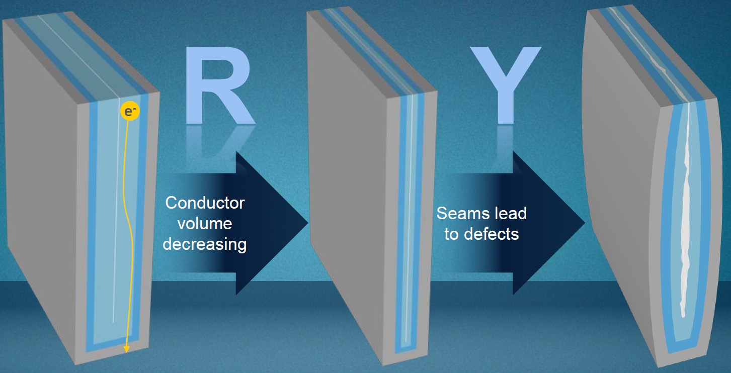
The biggest problem lately, however, is that the contacts have gotten skinnier and skinnier, making them more resistive because there’s just not much room left in the contact hole after the barrier and liner have been laid down. To the point where now the tungsten in the contact is the long pole in the tent: it’s more resistive than the silicide, according to AMAT. And it’s actually becoming a significant factor limiting the performance of the transistors being contacted.
But it gets worse. As the metal fills, it adheres not just to the bottom, but to the sides too. It fills from all directions, and, where it meets in the middle, there can be a seam. That seam can increase resistance and hurt yield.
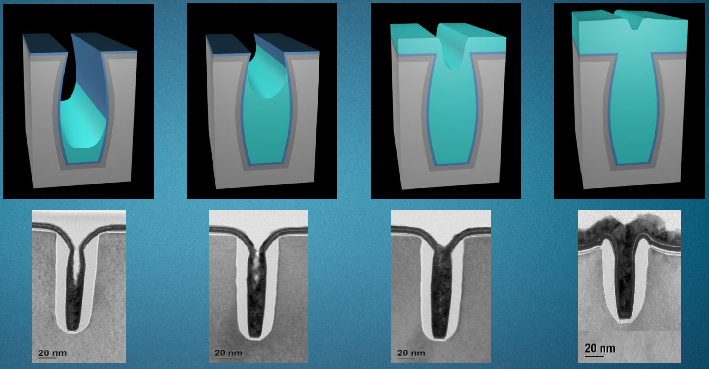
And then it gets yet worse. If the top of the contact hole is narrower than the bottom (or some inside part), then it’s referred to as “re-entrant.” (I have no idea why, but that’s what they call it. What are they re-entering??) So now, as it fills, the top pinches off first, and then nothing can get into the middle, which hasn’t finished filling yet. So you get a void. This is bad for resistance and bad for yield.
Yield is much more sensitive to failures at today’s nodes. AMAT didn’t have data specifically for contacts, but they did have data for vias, which illustrates the point (albeit possibly with different specific numbers). At 20 nm, 1 defect-part-per-billion (DPPB) can cause 30% yield loss. For comparison, it would take about 5 DPPB at 65 nm and 10 DPPB at 90 nm to cause that same yield loss. They don’t include numbers for truly aggressive nodes, like 10 nm. But you can well imagine that they’re not going to be better.
(Image courtesy Applied Materials)
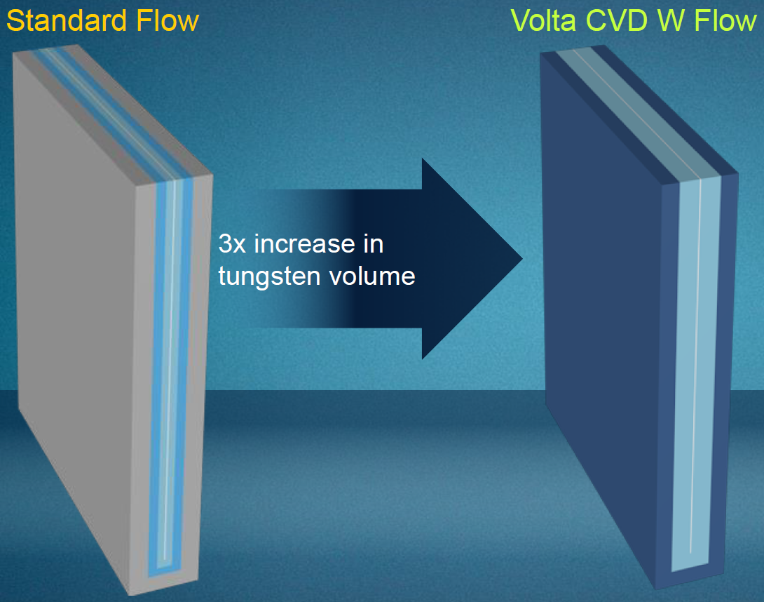
So they’ve done a couple of things to improve this situation. The first is to replace the barrier/liner layers with a single film. They’re not saying much about what this film is, other than that it’s a metal/organic-based tungsten film. It acts as both barrier and liner and, critically, has the thickness of only a single film.
They’re doing this via their Endura Volta system. The benefits are, first, that you’ve now got one layer instead of two; that simplifies the process. But, more to the point, because the barrier/liner combo is now thinner, it leaves more room in the cavity for the actual metal fill, reducing the resistance of the contact. (Yes, as things keep shrinking, we’ll eventually be back here again. We’re buying time. But that’s what the last 20 or more years have been, right? Buying time until CMOS finally dies as predicted decades ago?)
(Image courtesy Applied Materials)
After this, there’s another mysterious step they’re undertaking. It’s some kind of a treatment done to the inside of the liner. What it does is make it less likely that the metal will fill from the sides. In fact, the likelihood decreases as you move towards the top of the via.
So when you’re filling those re-entrant holes, pretty much nothing adheres to the top, and the opening stays open. The fill progresses from the bottom (OK, with a little meniscoid action up the sides), and only when it’s reached the top will it spill out of the opening. They accomplish this using their Centura iSprint system. (I can’t help thinking that the following illustration might have come from my last dental visit…)
(Image courtesy Applied Materials)
They refer to this as “seam-suppressed tungsten,” or SSW. (Yeah, that would actually be “seam-suppressed wolfram” if you’re being picky…)
So, at least for the time being, they claim a solution that will carry us forward for more nodes, reducing both contact resistance and yield-killing contact defects.
More info:
Applied Materials contact solution


What do you think about Applied Materials’ approach to aggressive-node contacts?