


The electronics and semiconductor markets have always been very competitive, and the ongoing consolidation trend has raised the stakes even higher. Additionally, significant investments must be made and requirements set well before the first unit ships. This up-front effort contributes significantly to the electronics value chain, where concepts and algorithms are invented and implemented as hardware or software. The hardware side is especially challenging due to its permanency and per-unit variable cost. The task of the hardware engineering team is to implement those concepts and algorithms in competitive and cost-effective silicon and to exhaustively verify that it will function as intended in every scenario.
Agility and Innovation
The value put into a new chip begins with an innovative concept that is designed to distinguish it from the competition. This innovation is typically one or more algorithms combined with some control logic. Often these algorithms are developed using MATLAB, by engineers that have little interaction with the hardware team.
A system architect deciphers these algorithms and decides how they can be implemented across hardware, software, and analog/RF electronics. At this phase, the algorithm may be refined further, for example modeling the fixed-point mathematical performance and exploring different implementation architectures for parts of the algorithm. Often Simulink is used for this purpose because it provides the necessary solver technology and architectural description methods to model electronics designs. MATLAB code may still be embedded in the simulation for the parts of the algorithm itself, or used for analyzing and visualizing simulation results.
At this point there is often a break in the flow; a specification document is written and provided to engineers responsible for the RTL coding, software coding, analog circuit design, verification, and implementation. The priorities at this stage are schedule predictability and risk mitigation, with a linear progression toward completion. However, in the complex world of electronics, change is inevitable; successful projects are the ones that can adapt to those changes.
Development agility signifies the ability to respond quickly and effectively to new information as it becomes available. That new information may come from outside, e.g. a changing market; or it may come from the project itself, e.g. a problem found in verification. A tightly-connected and optimized design flow is essential in order to be responsive to these inputs. Connections need to provide rapid, natural transitions that enable a design to not only move forward to the next downstream stage, but also accommodate iteration or backward steps to address required changes. A successful design flow needs to accommodate redesign.
The ability to innovate and the agility of the design process are inherently connected. Minimizing the time spent by the development team on automated tasks enables these scarce resources to spend more time adding value through innovation. Code generation technology provides a means to achieve this, and is the focus of the following sections.
Integration with Verification
Verification engineers are primarily responsible for ensuring that the final chip design functions as specified. Modern verification approaches utilize random and constrained random testing, where stimulus is sent into both the RTL design and a behavioral reference model where results are compared. This behavioral reference model is most often written by the verification team in parallel with the RTL development by the design team, both guided by the specification. Creating these behavioral models and then debugging them consumes valuable verification schedule time. If a mistake or omission exists in the manually-written specification, there is a risk of both models being incorrect which can cause a silicon re-spin; any change to the specification requires time to update both models.
A tighter, automated connection between the system/algorithm engineers and the verification team would eliminate the schedule inefficiencies and reduce the risk associated with writing and interpreting a specification. One approach is to co-simulate between MATLAB/Simulink and EDA simulators, but this does not scale for typical regression environments. A more scalable approach is to utilize automatic code generation to create a model that embeds the verified system-level algorithm as a golden reference in the verification team’s native environment.
Establishing this connection contains benefits for many kinds of verification environments:
- Digital components – eases the transition from directed testing toward model-driven verification approaches, such as constrained random. A behavioral model is required in order to generate the expected outputs for comparison in the scoreboard.
- Mixed-signal designs – the behavior of analog components can be captured in models along with behavioral models of the digital components. This enables simulators in both the analog and digital design flows to have visibility of the overall system behavior.
- SoC development – a virtual platform for early software development that requires SystemC/TLM models of new hardware IP.
A new capability exports MATLAB code and Simulink models to behavioral models with SystemVerilog/DPI or SystemC/TLM interfaces. For digital designs in MATLAB, the starting point is a MATLAB function. For digital or analog/mixed-signal designs in Simulink, the starting point is a Simulink subsystem.
MATLAB Example: Exporting a Digital Model to SystemVerilog with DPI-C
A MATLAB function calculates an FFT of a complex input vector then compares this reference output with the implementation results. The entire function is generated as C and wrapped in a SystemVerilog module using DPI-C. This generated module can then be included in a SystemVerilog-based verification environment, e.g. as part of the scoreboard in a UVM framework.
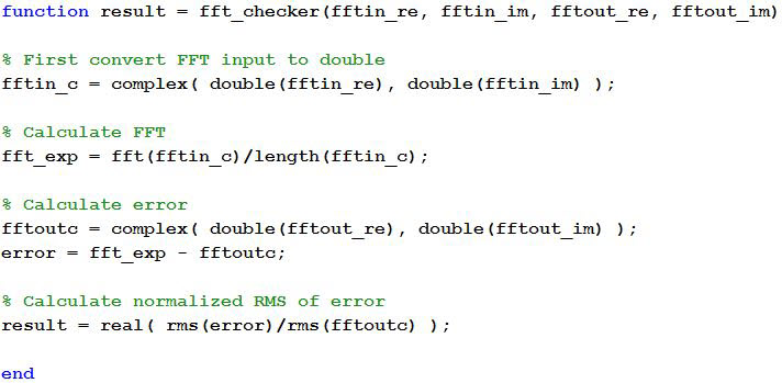
Figure 1. MATLAB code for FFT checker.
The dpigen function provided by HDL Verifier uses MathWorks’ C code generation to generate a SystemVerilog DPI component.
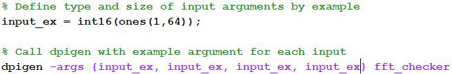
Figure 2. dpigen function usage.
This generates C code for the MATLAB function, DPI wrapper, and SystemVerilog declarations, and calls a Makefile, building it automatically. This component can now scale easily for use in verification environments where multiple parallel simulations are launched across large compute farms.
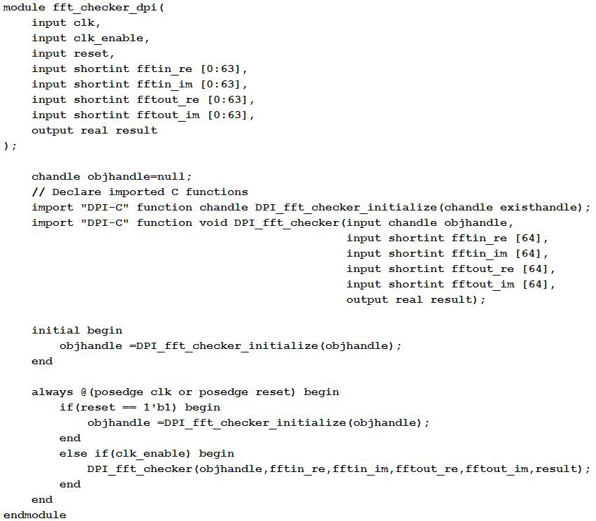
Figure 3. Generated SystemVerilog module.
Simulink Example: Exporting an Analog Model to SystemVerilog with DPI-C
Simulink is a behavioral-level simulation environment that enables system architectures and design alternatives for analog/mixed-signal designs to be explored and evaluated quickly before moving down to the slower circuit-level. The components from both the analog and digital parts of the design in Simulink can be exported to the circuit simulation environment as fast-running behavioral SystemVerilog DPI-C components.
The following example generates a SystemVerilog/DPI-C model of the front end anti-aliasing filter of an ADC in Simulink.
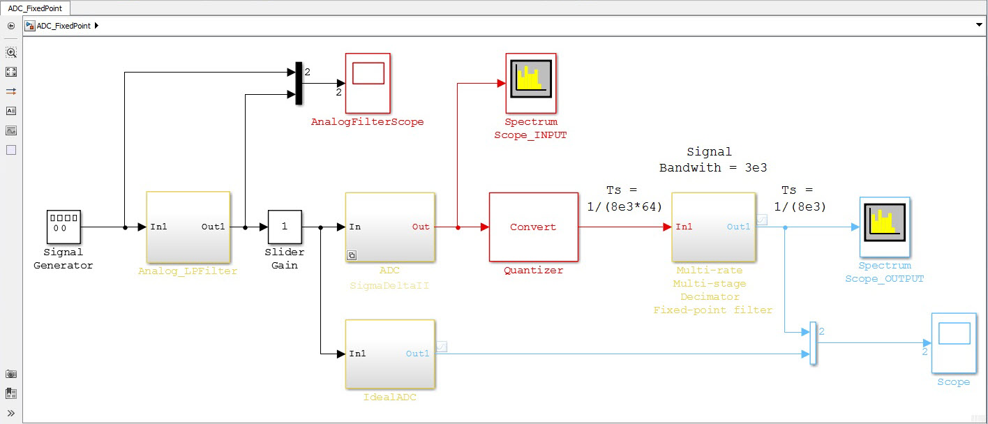
Figure 4. ADC model in Simulink.
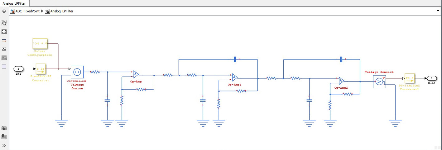
Figure 5. Detail of analog filters with analog circuit description.
Simulink provides variable-step solver technology, which is efficient for simulation of circuits. However, as you are translating this to C code, which will be scheduled externally, you need to use a solver that updates at a predetermined rate. When converting to a fixed-step solver, it is important to verify the choice of update rate to achieve your desired level of simulation precision. Tools provided with Simulink can speed this analysis by visualizing the differences along with relative and absolute tolerances.
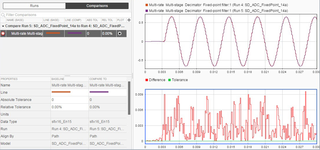
Figure 6. Comparing results from multiple simulations.
Once satisfied with the accuracy of the simulation, under the model’s code generation options, you specify SystemVerilog DPI-C export:
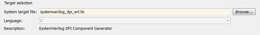
Figure 7. Selection of SystemVerilog target in code generation options.
Clicking “build” on the context menu of a relevant subsystem generates the DPI component in the same format as previously shown with MATLAB.
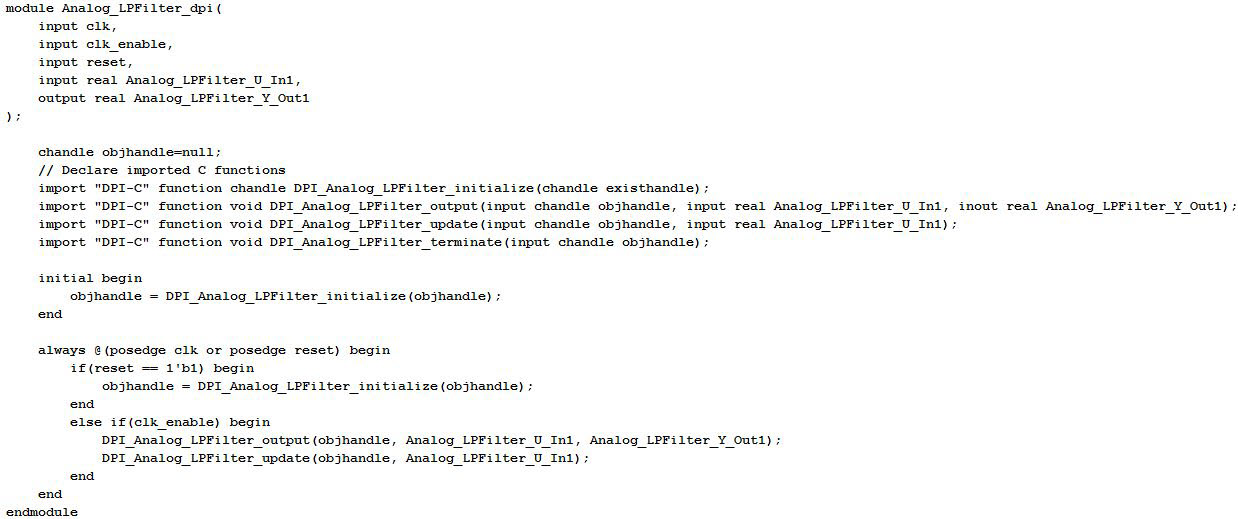
Figure 8. Generated SystemVerilog module from Simulink.
Integration with Implementation
Digital hardware design engineers read the specification and write RTL code to begin implementation. Hardware designers add value through their expertise at implementing micro-architectures and understanding how it synthesizes to physical hardware resources. Manually writing RTL to perform this task severely limits the ability to explore the range of micro-architecture possibilities and increases the introduction of bugs that must be identified and remedied during verification.
With HDL Coder, the hardware engineers can collaborate with the system and algorithm engineers in MATLAB and Simulink to refine the algorithm design toward an implementation model. This includes: designing the hardware architecture into the model, converting floating point data to a fixed point, applying settings to specify where to apply optimizations (such as resource sharing or pipelining), then finally, generating the RTL. The result is often a more optimal implementation due to the ability to explore a broader solution space. Since RTL can be quickly regenerated when changes are made, the RTL is always functionally in sync with the system design.
By focusing efforts on the value-add activities and automating wherever possible the procedural task of writing the bulk of the code itself, the value and productivity of hardware engineers increases dramatically.
Example: Translating MATLAB and Simulink models to Verilog
In the following example, a Simulink model describes the architecture of an 8-tap symmetric filter design, with resource sharing applied to minimize the amount of physical hardware required. This employs the reuse of a single component with pre-adder, multiplier, and adder for accumulation of the result.
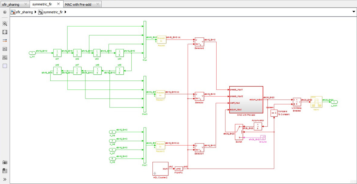
Figure 9. Model refined with implementation architecture detail.
The generated Verilog from this model respects the architecture of the original model while minimizing the area through reuse of resources at a higher clock rate. The detail of this shared component, and the Verilog generated from that part of the model, is shown below.
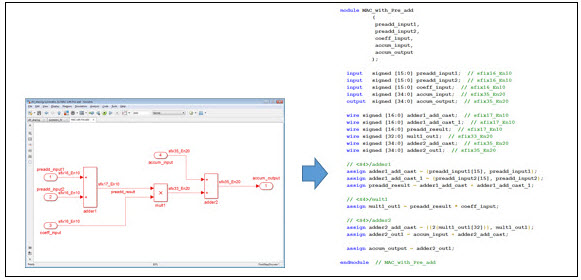
Figure 10. Automatic Verilog code generation from Simulink.
Managing the Design Flow
Optimizing the design flow increases competitive advantage, but making changes must be managed carefully to minimize disruptions. In this case, a natural first step is to begin with verification. Since the purpose of a reference model is to accurately represent the functional behavior of the algorithm, directly generating a SystemVerilog DPI-C component from the model itself saves the verification team time; only one model needs to be created manually from the specification reducing the likelihood of errors.
This also facilitates collaboration between the system and verification teams. The algorithm model becomes useful beyond the system team and becomes a deliverable. More effort is invested to ensure the functionality is well-described and well-verified at this early stage through increased testing, coverage analysis, and formal methods, which will further reduce the load on the verification team.
Adopting code generation for hardware implementation will be more disruptive, as the hardware engineers will need to learn how to use new tools to express their architecture decisions and generate RTL of the quality to which they are accustomed. For this reason it is typical to start with a small algorithmic component and a few individuals on a project. Further additions can be made once project members understand how to successfully share experiences with other users in the organization.
Finally, the organization needs to embrace this new collaboration and understand the objective; each user should feel comfortable contributing their unique value toward the greater sum of the group.
Summary
Communication across the design flow is key to enable an agile development process. That communication starts with the conceptual algorithm design, and continues through to the verification of the silicon itself. To bridge the gaps in this flow, teams need to communicate and utilize an integrated set of tools. With many of today’s semiconductors containing innovative algorithms that begin life in MATLAB models, MathWorks has developed capabilities that enable these models to be shared and reused in the later stages of the design flow. This includes not only the generation of implementation code, but also the generation of verification models for use with SystemVerilog environments. As verification is the biggest cost in a typical semiconductor design cycle, it is a great place to start deriving further efficiency.
Authors:
Graham Reith, MathWorks, Cambridge, UK (graham.reith@mathworks.co.uk)
Jack Erickson, MathWorks, Natick, Massachusetts, USA (jack.erickson@mathworks.com)


6 thoughts on “System-wide Collaboration”