


Editor’s Note: While Amelia’s Halloween Fish Fry had us all running out and gleefully building our own singing Tesla coils, and even though shuffling quietly across the carpet and sending a bright 10,000-volt arc from your fingertip to a napping family member can be a barrel of laughs, there are times where we most definitely do not find electrostatic discharge so amusing. The first of those, of course, is when we ARE the sleeping family member. Sheesh, what an insensitive prank!
But, a second scenario where we do not welcome the effect of high-voltage static discharge events is when we’re designing high-speed communications circuits. Getting your Ethernet port zapped with a 10kV ESD is far from fun – especially for the Ethernet port. But, how do we help our circuits protect themselves? Ian Doyle of ProTek devices has some very helpful suggestions.
–Kevin Morris, Editor-in-Chief
————————————-
Transmission data rates continue to grow and grow to meet consumer demands for multimedia rich content, such as streaming video. In turn, whether in the home or at the backend, Ethernet connectivity also continues its widespread use. As a result, and more than ever, electrostatic discharge (ESD) transient threats pose challenges to system designers to incorporate overvoltage protection that doesn’t impact performance.
The International Electro-technical Commission (IEC) has defined a Human Body Model (HBM) ESD event. The intent is to guide designers in implementing adequate protection in their electrostatic applications. The IEC defined the HBM ESD discharge impulse, with four levels in standard 61000-4-2. It has a rise time of less than 1 ns and decay time of 60 ns.
As a system requirement, the four levels of IEC 61000-4-2 cover up to ±8 kV contact / ±15 kV air discharges for ESD transients in systems. In some applications a higher level is specified for enhanced contact and air discharge specifications. This is because human body models can reach ±25 kV in static-rich environments.
Ethernet Port Protection
When specifying protection levels for Ethernet ports, the first protection device to consider is the use of a transformer. The transformer provides interface isolation along with the termination capacitor between the drive circuitry and communication lines. The Rx and Tx signals are normally transformer coupled. The “Bob Smith” termination originates from his US patent 5321372 Apparatus and method for terminating cables to minimize emissions and susceptibility.
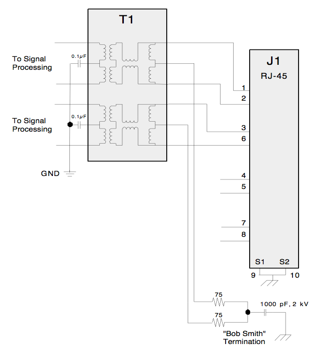
Ethernet Port with Isolation Transformer
IEEE standard 802.3TM-2005/Cor 1-2006 states that the electrical isolation shall withstand at least one of the following electrical strength tests:
- 1500 Vrms at 50 Hz to 60 Hz for 60s, applied as specified in sub clause 5.2.2 of IEC 60950-1:2001.
- 2250 V dc for 60s, applied as specified in sub clause 5.2.2 of IEC 60950-1:2001.
- A sequence of ten 2400V impulses of alternating polarity, applied at intervals of not less than 1s. The shape of the impulses shall be 1.2/50µs (1.2µs virtual front time, 50µs virtual time of half value), as defined in IEC 60950-1:2001 Annex N.
It is defined in sub clause 5.2.2 of IEC 60950-1:2001 that during the test there shall be no insulation breakdown. The resistance after the test should be at least 2 micro ohms, measured at 500V dc.
Protecting the Secondary-Side of the Ethernet Transformer
If the Ethernet transformer can support the impulse tests without failure, protection will only be needed on the secondary side of the transformer. This is to protect the Ethernet IC from the energy transfer before the transformer saturates. A typical Ethernet transformer can withstand 200-300 A 2/10?s before failure occurs, but this needs to be verified by testing. The secondary protection solution needs to ensure it can support this energy – including ESD and surge transients – without letting through too much voltage that would overstress the IC.
A bridge diode network clamps any positive or negative transients to the power supply lines. Therefore, the line driver outputs are limited to an overstress of the forward voltage of the diode under impulse. Diode manufacturers do not specify the forward voltage under the common telecom impulses which makes product selection difficult. Diodes that offer low VF voltages under fast transients are important to limit the stresses on the Ethernet driver. As a “rule of thumb,” electronics engineers can use as high an IF rating as possible and select ultra-fast diodes to ensure stresses are kept to a minimum. The energy is also transferred to the power supply. Designers should be aware if high efficiency (low quiescent current) line driver components are used. This can have the effect of increasing the supply voltages as the load regulation capacitors absorb the energy. The DC/DC converters used to generate the power supply cannot sink current and therefore will stop regulating if the voltage gets too high. This can make the supply lines become unregulated for a short period of time, which can damage ICs.
It is important that industrial application designers understand that their solutions are likely to be exposed to external ESD, EFT, surges, lightning or improper wiring during installation. This includes ESD levels per IEC 61000-4-2 and EFT levels per IEC 61000-6-4. Critical systems and integrated circuits (IC) will be exposed to such elements and designers should remember that devices may not be resettable and may be damaged beyond repair.
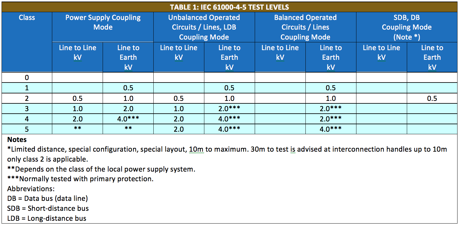
For surge protection per IEC 61000-4-5, it is critical for the design engineer to understand what installation classification is required for a system. They include:
- Class 0: Well-protected electrical environment, often within a special room.
- Class 1: Partly protected environment.
- Class 2: Electrical environment where the cables are well separated, even at short runs.
- Class 3: Electrical environment where cables run in parallel.
- Class 4: Electrical environment where the interconnections are running as outdoor cables along with power cables and cables used for both electronic and electric circuits.
- Class 5: Electrical environment for electronic equipment connected to telecommunication cables and overhead power lines in a non-densely populated area.
Once the classification is known, the level of protection required can be determined using the IEC 61000-4-5 test levels, as shown in the below table (click image to enlarge).
Recommended Solutions
A design engineer could use two low capacitance, low clamping voltage steering diode / transient voltage suppressor (TVS) arrays for high speed interfaces such as GbE ports. Designers can implement the slower 10/100 speed configuration using a single steering diode / TVS array device.
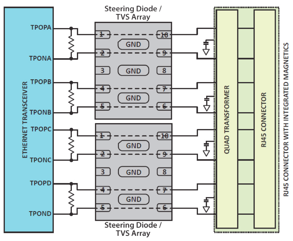
Fig. 1: Implementation of two steering diode / TVS array devices for circuit protection on secondary side of LAN transformer in Ethernet GbE interface application
By using a proper device that meets international standards, such a configuration provides the following benefits:
- ESD protection per IEC 61000-4-2 (±8 kV contact / ±15 kV air discharge)
- Electrical fast transient (EFT) protection per IEC 61000-4-4 (40 A 5/50 ns)
- Surge protection per IEC 61000-4-5 (24 A 8/20us level 2 (line to gnd) Level 3 (line to line)
The circuit protection components in use should also ensure several capabilities:
- Low threshold voltage rating of 2.5 V to match low voltage PHY chipsets
- Low line capacitance of 3.5 pF for transmission rates
- Low leakage current 0.5 uA @ 2.5 V for good energy efficiency
- Low profile packaging to save on real estate for high speed interface and PCB applications
Layout Considerations
For transients to affect the power supply input/output of an Ethernet data line controller, or other data lines for this matter (USB, HDMI, etc.), the transient must be in between the power line and system GND. Therefore, the protection device should be placed between the two connector terminals as close as possible to the external connector. Most portable equipment have only a system ground where the overvoltage protector will shunt the excess energy. This causes the whole system to be affected by the loop current and can cause ground bounce due to the inherent inductance in the PCB tracks.
Inductive reactance is defined by the equation, XL = 2?FL. Here, high frequency signals (HBM ESD equal to less than 1ns rise time) will effectively increase the track resistance and therefore the voltage across it with the transient current. The inductance reactance can also be used as a benefit by further reducing ESD damage from reaching critical components. The impulse can be significantly reduced by placing the protector as far away from the IC as possible to provide additional series inductance between the two components. High voltages (6kV or more) entering the board can cause flashover onto adjacent tracks. Therefore, the overvoltage protection device should be located as close as possible to the connector where the ESD transient could enter the system.
The protection device should be placed as close as possible to the communication lines where ideally the protection device termination pad should be integrated directly onto the communication line. Having interconnects from the communication line to the protector introduces additional inductance and impedance mismatches. This track inductance becomes a hindrance as it is now in series with the diode or varistors. This has the effect of increasing the initial overshoot of the device. IC manufacturers discourage long track lengths between the connector and the IC as this can be deleterious to performance. Therefore, it is key to select a good quality overvoltage protection device that has low trigger voltage, low overshoot and low clamping voltage performances.
As mentioned, Ethernet continues to be a widely deployed and used technology. In fact, a presentation by the Ethernet Alliance illustrates Ethernet port shipments grew from some 200 million in 2004, to around 300 million five years later in 2009, to more than 400 million in 2012. The presentation also illustrates how standardized link speeds continue to grow, from 10GbE around 2004, to 40 GbE around 2009, to 100-400 GbE today. This usage is to support growing consumer demand for rich and reliable multimedia content. As a result, system designers are challenged more than ever with incorporating overvoltage protection that does not degrade transmission rates.
About the Author: Ian Doyle is the director of EMEA sales and marketing for ProTek Devices. The company provides circuit protection solutions for applications such as telecom, industrial, consumer, military, aerospace, medical and instrumentation. Doyle holds a patent for a simplified sub-harmonic I/Q modulator and has other CPD qualifications in RF/MW design, IT, sales and project management. Prior to ProTek Devices he worked at PLM Semiconductors where he had global product management responsibility for the company’s transient voltage suppressor (TVS) diodes, TISP® Thyristors and TBU® (Transient Blocking Units). Before this, starting in 1998, Doyle worked at Bourns, Inc. with roles in global application engineering, product development and product line management. Doyle received a bachelor’s degree in engineering (electronics) from the Cork Institute of Technology, Ireland.


8 thoughts on “Overvoltage Protection in High Speed Communication Ports”