


Circuit reliability verification has become a crucial step in IC design. Reliability requirements are not only growing in all market segments, including automotive/transportation, medical, mobile/wireless, and consumer electronics, but the complexity of today’s circuits is presenting unprecedented verification challenges. To get these designs to market in a timely manner, while ensuring they will perform as designed, designers need automated circuit reliability solutions that can quickly and accurately analyze these complex designs.
From the designer’s perspective, two critical factors in efficient reliability verification are:
- the ability to understand the logic of the circuit
- the ability to recognize specific circuit topologies (patterns) associated with circuit reliability
The second factor, pattern recognition, is particularly useful for application conditions such as electrostatic discharge (ESD), electrical overstress (EOS), low/multi-power designs, and latch-up, among others. Automated pattern recognition capability can enable designers to find and analyze specific design patterns of interest (for instance, ESD protection schemes, or level shifters) quickly and efficiently. For ease of use, as well as broad applicability, designers need both the flexibility to define these patterns in a simple way (e.g., SPICE) that is independent of the design cell names, and the ability to define some margin around a design pattern, so that similar, but not exact, matches can be identified for analysis when appropriate.
Design Pattern Usage
ESD Protection
ESD causes severe damage to ICs, but installing ESD protection circuits where necessary can mitigate or eliminate the risk of ESD. Because checking for proper ESD protection circuits is critical for reliable designs, several protection schemes already exist [1] [2] [3]. The design rules focus on verifying the presence of the appropriate protection schemes from a topological perspective, but designers must verify the appropriate protection on both the schematic netlist (early in the design cycle) and the layout netlist. Designers must also perform checks on circuitry directly connected to IO pads, as well as checks on the ESD network. Figure 1 demonstrates some examples of ESD protection circuits.
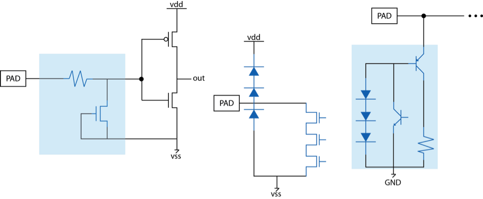
Figure 1: Sample ESD protection circuits
Using circuits similar to these as models, designers can develop patterns for ESD protection circuitry using the SPICE format. Once a pattern is defined, automated circuit reliability verification tools can quickly check for and verify that pattern everywhere it is used in any design. From the designer’s perspective, using patterns simplifies the task of switching between different protection schemes, and enables designers to easily define complex structures one time for repeated use. Designers only need to:
- Identify the protection schemes
- Write a SPICE pattern template (used as an input for the circuit verification tool) for each protection scheme
- Run the circuit reliability tool to automatically identify pattern violations in a design
Let’s look at how to perform this verification methodology, using a simplified example (Figure 2) to clarify the process. The design team identifies the two ESD protection schemes that should be used in the company’s designs, and determines that they are represented by the two ESD topologies shown. The next step is to write SPICE pattern templates that describe these protection schemes as SPICE sub-circuits. Once the template is created, the user can write a simple rule file that points to this template and instructs an automated circuit reliability verification tool to verify these patterns on all IOs in the design. Designers can then run the circuit reliability verification tool against a design to automatically catch any protection circuit violations. In our example, the tool found an IO pad with no protection at all.
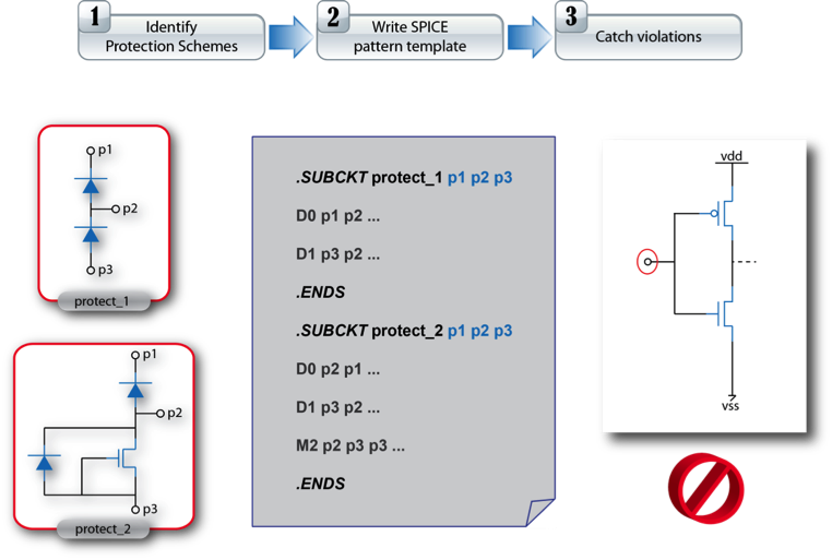
Figure 2: Circuit reliability verification using pattern recognition methodology
Using this SPICE pattern template methodology allows design teams to easily add or remove protection schemes to the template, based on the methodology applied by the company for ESD protection.
In the real world, of course, designers also need the flexibility to deal with potential variations in each protection scheme by providing some defined margin for the matching process. Actual topologies are not always an exact match to a pattern, but designers can’t define a pattern for every possible combination to cover all scenarios. That approach would be exhaustive, time-consuming, and might even lead to missing some real scenarios. For example, a protection scheme may require a protection diode between the IO pads and power/ground with certain connectivity. However, in real designs, this “diode” may actually be a series of diodes. Allowing for a controllable margin in the matching process not only simplifies the designer’s task, but also enables a wide range of valid circuit configurations to be verified quickly and easily.
Figure 3 illustrates an example of design variations that designers have to deal with, and demonstrates how designers can manage these variations efficiently from the pattern template. As shown, there is a defined ESD protection scheme using two diodes. The up diode is between the IO pad and Power pad, where the positive pin is connected to the IO pad and the negative pin is connected to the power pad. The down diode is between the IO pad and Ground pad, where the negative pin is connected to the IO pad and the positive pin is connected to the ground pad. Using the pattern template, the designer defines a SPICE pattern to describe this protection scheme (protect_1).
If the designer tried to match this exact pattern to the three designs in the figure, there would be only one match, because one of the designs has the up diode formed as a series of two diodes, while another uses a series of three diodes. Verification can be greatly simplified if the reliability verification tool can allow for variants on the specific circuits. Here the designer has defined an optional configuration permitting the up diode device to be a series in the pattern template. By making the template more flexible, the designer can now match the protection scheme efficiently and accurately on all three designs. While the technique for specifying margins may vary between tools, the ability to allow for pattern variation is essential to an effective automated pattern recognition process.
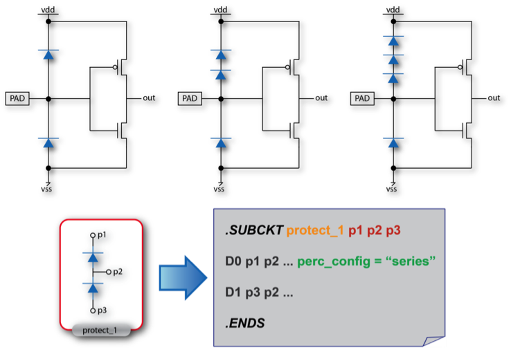
Figure 3: Flexibility in Pattern Recognition (code source: Calibre PERC)
Low/Multi-Power Designs
Another important application for design patterns is in low/multi-power designs. The complexity of system-on-chip (SoC) designs is increasing, with more analog and digital circuits being integrated on the same chip. Mixed-signal designs require different voltages to support each power domain on the chip. ICs with multiple power domains have signal lines that must cross from one domain to another, and these crossing points are often a point of failure or damage. Designers must design appropriate protection schemes using level-shifters to control the voltage shifts, and insert them at these crossing-domains interfaces. If the design moves from a low-voltage domain to a high-voltage domain without a low-to-high level shifter the design cannot drive the high-voltage domain circuitry to work. If the design moves from a high-voltage domain to a low-voltage domain without a high-to-low level shifter, the design will over-drive the low-voltage domain circuitry, leading to device damage over time. There are several types of protection schemes used to avoid power domain failure conditions [3] [4] [5].
For example, designers must verify that the appropriate level-shifter is used at each domain interface, and that it is correctly connected. However, design methodologies often don’t have a naming convention for level-shifter cells, or the level-shifter is formed from multiple cells. Because of this, the designer must verify the appropriate level-shifter existence based on its topology (circuitry), instead of a cell name. By using pattern recognition functionality, designers can define all their level-shifter configurations/circuits in a SPICE format in the SPICE pattern template, then use this as an input to the circuit verification tool to automatically find all level-shifters and identify any errors. As in our previous example, designers need some flexible margin that can be applied during matching to find similar, but not exact, matches.
Figure 4 demonstrates a simplified example of level-shifter protection and how designers can use the pattern recognition functionality to efficiently manage level-shifter checking. There are two different voltage domains, so a level shifter is required between the domains. The design contains a cell (“LS”) between the two different domains. However, this cell name does not tell the designer if this is the correct level-shifter for this location, or if the level-shifter is accurately configured. With design pattern recognition, the designer can write a SPICE pattern template with all level-shifter configurations as SPICE sub-circuits, and assign each one a user-defined name to indicate its function. In this example, “level_shifter_LH” defines a SPICE configuration for a low-to-high level-shifter, and “level_shifter_HL” defines a SPICE configuration for a high-to-low level-shifter. The designer can also define some variation margin (using the “parallel” and “series” options) that can be applied during pattern matching to find similar topologies. As before, this example uses code from Calibre PERC—other tools may implement these configuration definitions slightly differently. With these pattern definitions in place, the designer can run the circuit reliability verification tool to automatically determine if the “LS” cell is really the appropriate level-shifter for that location and that it is accurately configured.
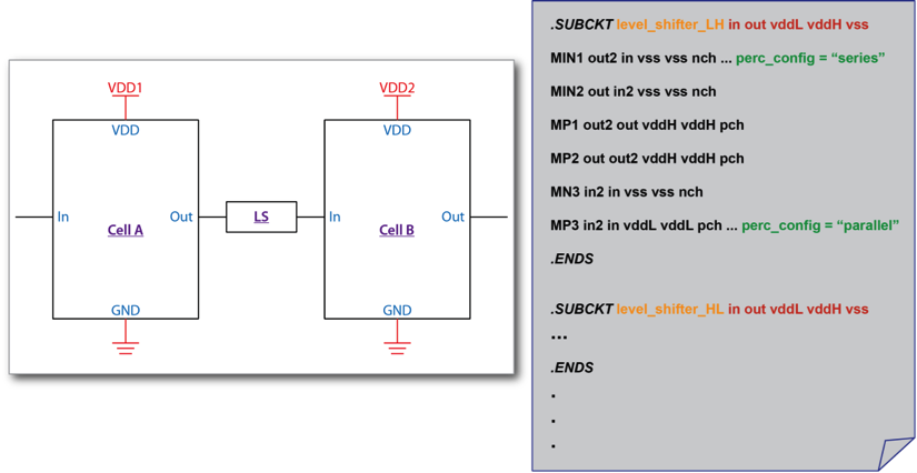
Figure 4: Pattern Recognition for Low/Multi-power designs (code source: Calibre PERC)
Conclusion
Using design patterns to ensure circuit reliability is a critical skill for all designers working at advanced nodes. With today’s complex designs, the ability to pre-define complicated topologies and confirm they are properly implemented in a design is critical to meeting both time-to-market schedules and reliability requirements. Combined with new circuit reliability tools that provide automated pattern matching and analysis, design patterns enable fast, efficient circuit reliability verification.
References:
[1] Muhammad, M.; Gauthier, R.; Junjun Li; Ginawi, A.; Montstream, J.; Mitra, S.; Chatty, K.; Joshi, A.; Henderson, K.; Palmer, N.; Hulse, B.; , “An ESD design automation framework and tool flow for nano-scale CMOS technologies,” Electrical Overstress/ Electrostatic Discharge Symposium (EOS/ESD)
URL: http://ieeexplore.ieee.org/stamp/stamp.jsp?tp=&arnumber=5623716&isnumber=5623704
[2] Mauro Fragnoli, Eleonora Gevinti, Antonio Bogani, Lorenzo Cerati, ” Novel initialization and implementation method for HBM ESD compliance automated check on Smart Power IC’s”, DAC User Track, 2012 URL: http://www.dac.com/conference+program+user+track.aspx?event=334&topic=8
[3] Jerome Lescot, Vincent Bligny, Dina Medhat, Didier Chollat-Namy, Ziyang Lu, Sophie Billy, Mark Hofmann, “Static Low Power Verification at Transistor Level for SoC Design,” ISLPED 2012, July 2012 URL: http://dl.acm.org/citation.cfm?id=2333694
[4] Dina Medhat, “Power-Aware Verification in Low-Power ICs”, Chip Design magazine, Fall 2012
URL: http://chipdesignmag.com/display.php?articleId=5163
[5] Dina Medhat, “Easier Cross-Domain Signal Protection for Mixed-Signal SOCs,” EE Times, December 2009 URL: http://www.eetimes.com/document.asp?doc_id=1276206
About the Author:
Dina Medhat is a senior technical marketing engineer for Calibre Design Solutions at Mentor Graphics. She has been with the company for eight years. Dina holds a BS and an MS from Ain Shames University, Cairo, Egypt. She may be contacted @ dina_medhat@mentor.com


Mentor’s Dina Medhat has described how pattern matching can help improve the reliability of your circuits. What do you think?