


There’s a scramble afoot as sensor and silicon and software and system folks try to jockey over the best way to implement and integrate sensors into a broad range of devices. You’ve got:
- Folks making sensors
- Folks making micro-controllers that can run sensor-related software
- Folks integrating sensors and micro-controllers together
- Folks integrating multiple sensors together in a single package, possibly with a micro-controller as well
- System guys controlling sensors via the AP in an SoC
- System guys including a sensor hub of some sort in an SoC
The variations seem endless. Part of it is the natural thrash of a new market where everyone is trying to leverage their own core strengths to bend the market their way. But it’s also driven by the fact that no one solution is right for the variety of applications in smartphones, tablets, fitness gadgets, industrial implementations, and the other wide-ranging applications involving sensor swarms and the Internet of Things.
And most of the players here have been members of the sensor ecosystem. But as implementation starts to impact SoC design, then pieces of the sensor support infrastructure become IP that needs integration into a larger silicon design, and that necessarily grabs the interest of EDA folks who might not have had a visible presence to date.
So, while it was surprising to hear Synopsys making a sensor-related announcement, in retrospect, it shouldn’t be. They’re obviously a huge name in the digital logic implementation and timing realm, and they are one of the largest providers of silicon IP. So I’m sure their ears have perked up over the last few years as they’ve watched what’s happening.
And the product of that heads-up was announced a few weeks ago: a sensor subsystem framework. While this isn’t about integrating actual sensors onto an SoC – that would take some major cojones given that even integrating a sensor with a CMOS conditioning chip is not typical – it is about integrating as much as possible into an SoC.
That means you need:
- A way to attach to the sensors.
- A place to execute fusion software.
- Connectivity to a host processor.
- Memory and interconnect to allow efficient data management.
- Access to computation accelerators like floating-point engines or hardware offloads.
The thing is that each system that includes such a subsystem will be different. So this isn’t about a fixed configuration; it’s about providing a scaffold onto which the necessary pieces can be hung. And making it easy to do that.
Part of the problem is that sensors have become interesting to more than just sensor experts. Everyone wants one, but no one wants to have to become an expert in the nuances of sensor magic in order to leverage their benefits. So abstraction and encapsulation are important to this sort of strategy, while leaving room for Power Users to get in and add their own special sauces.
So here’s what Synopsys has pulled together. The central hub of their subsystem comes courtesy of their ARC acquisition. It acts as a dedicated low-power sensor management unit. It communicates with the host CPU via a variety of possible interfaces – even JTAG. (I’m going to assume that’s only for debug and diagnostic purposes…)
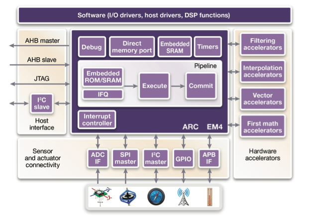
Courtesy Synopsys
Communication with sensors themselves can be through the typical lower-level protocols or I/Os; whichever ones used will be driven by what the sensors themselves require. Many sensors are digital now, perhaps even with some low-level fusion providing higher-level results like orientation. But some are analog, meaning that an ADC interface is required.
Note that the ADC itself isn’t part of the framework. That’s because this subsystem is process-agnostic and synthesizable, while ADCs are process-specific hard IP. The ADC may reside on the SoC, but it would be included as a separate piece of IP outside the scope of the sensor subsystem, and it would then be connected to the subsystem through the ADC interface.
Then there is the option of using hardware accelerators. And this gets interesting because it’s one area where a designer could get thrown into a nasty pit of details that they don’t really want or weren’t anticipating.
Abstracting things like sensor fusion means burying the low-level details like the specific math used to calculate orientation. If you’re designing a smartphone SoC, you probably don’t want to be drawn into the details of Kalman filtering. Sensor fusion IP can eliminate the need for knowing these details if you don’t want to.
But what if the software runs too slowly? What if you want to use an accelerator? Well, now you need to know where the bottleneck is and what to accelerate, which can rapidly suck you into knowing more about the fusion algorithms than you wanted. Sinking too deep is somewhat mitigated by a broad library of functions both in software and in hardware, but even that could drag you off into the weeds.
Synopsys shows a simple example of a square-root function, available from their libraries. Conceptually, things are simple: an all-software implementation takes 353 cycles to execute and requires no hardware area other than the processor on which it’s running (which can be reused for lots of things). A full-up hardware accelerator can do the job in 6 cycles, but it needs almost 5500 gates to do the job. A hybrid approach can still complete the operation in 24 cycles with the addition of only 1075 gates. You might consider this to be an optimal point.
Synopsys allows you to dial up how much hardware acceleration you want – but this would seem to place the burden on the designer of knowing how the function – square root, for example – is implemented, the various algorithm options, and how they lay out in software or hardware. That’s not going to fly. On the other hand, it’s hard to imagine a generic “wizard” that can let you dial up infinite gradations between hardware and software on any given piece of IP.
What Synopsys has done is to take something like a square root function and create a variety of implementations – from all software to all hardware and one or more points in between. They’ve then documented the performance and area implications. So while you don’t have a dial with infinite settings, you do end up getting a list of choices: you can pick the one you want without having to know in detail how each one is optimized or implemented.
All of these pieces can be assembled using a drag-and-drop interface where you can tell the tool what you want and specify any options.
Above all of this is a layer of software including drivers of various sorts and DSP functions. This allows software writers to focus on their actual applications rather than the plumbing required to get their apps to talk to the sensor subsystem.
The benefits they claim by putting all of this together are 40-60% reduction in area – down to as low as 0.01 mm2 in a 28-nm process; lower latency; and lower power – can be less than 4 µW/MHz in 28 nm. Design goes faster because the pieces already exist; verification goes faster because everything has been pre-verified. Software can be implemented more quickly because drivers and such already exist.
So Synopsys is clearly trying to insert themselves into the picture here by doing a lot of the work that system designers don’t want to do. It leaves lots of software flexibility – the code isn’t closed – but then you can also choose to accelerate if needed. My suspicion is that for the general case, hand-holding might be needed, but if it all fits together as promised, that’s still easier than having to gin it all up from scratch.
More info:


What do you think of Sysnopsys’s sensor subsystem?
Sounds like what IBM has done in the 60s with its 360/370 series mainframes: Scalable Architecture.