

We looked at extreme ultraviolet (EUV) lithography a short while back, but I intentionally glossed over one important aspect: the source of the EUV energy. This is a topic worthy of attention on its own, as there have been years of research on this – and some recent developments that may take it in a new direction. And, I don’t know, it’s kinda cool.
EUV means high energy, so you’ve really got to rattle the crap out of some kind of material in order to get it to shed high-energy photons. We’re not just talking boiling or barbequing; we’re talking plasma. And the catch is, this isn’t simply shooting a few photons at some film like your dentist does (with X-rays, which are even higher-energy). As we saw before, the real challenge here is more power so that more wafers can be exposed more quickly.
There are two fundamental approaches that have been taken to getting materials to shed energy in the EUV range. The first is called discharge-produced plasma (DPP). With this approach, you take a low-temperature plasma and pinch it magnetically to get a high-temp plasma. The other approach is called laser-produced plasma, or LPP. In that case you bombard some target material with a laser.
An important measure of the effectiveness of a system is the conversion efficiency (CE). This is, simply put, the ratio of the EUV energy you get out of the system divided by the energy used to produce the EUV. The numbers aren’t high – less than 10%. With DPP, it might even be overstated, since, depending on the source of numbers, its CE apparently might not include the energy required for the electrical support system. In general, it’s said to be easier to convert “wall power” to a laser pulse, so the overhead for LPP is usually lower.
Typical materials used, at least in research, have included xenon, tin, and lithium. Xenon generally gives a low CE; it simply takes too much energy, particularly for cooling, with DPP. You can’t even get a laser strong enough to use LPP with xenon (and, I’m no expert, but shooting a laser into a gas just doesn’t feel like it would be very efficient…).
Lithium has a CE range of 2-3; tin has a theoretical CE of 4-7.5% or so. With LPP, tin has the additional issue of creating debris that can mess up the optics, which you may recall are all mirrors instead of lenses. That creates a maintenance and wear-out issue.
These two approaches have dominated the research papers for the last several years, but at Semicon West, Xtreme Technologies presented a third alternative that they call Laser-assisted Discharge Plasma (LDP). As the name might suggest, they claim that this approach combines elements of their learning from both LPP and DPP.
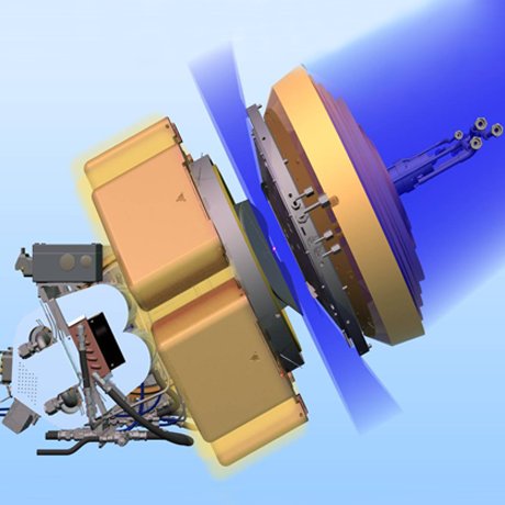
The mechanical arrangement of LDP departs significantly from that of its forebears. It consists of two counter-rotating wheels, dipped into a liquid tin bath. The wheels effectively form a pinch point at the location of closest proximity. The rims of the wheels get coated with liquid tin, and that tin is hit by a laser on one of the wheels right at the pinch point. That creates a discharge across to the other wheel, and that discharge generates the EUV photons.
There are a number of things going on here that work together to satisfy the many elements that must fall into place for a system like this to function properly, and the liquid tin plays most of the roles. First, you need electrodes for the discharge: the liquid tin acts as the electrode on both sides right at the pinch point.
Second, in order to get an arc across the gap, you must have a field. That field is created by a power source that energizes the two liquid tin baths. This builds a complete circuit from bath-to-rim-to-spark-to-rim-to-bath (the green path in the figure).
Third, this stuff gets hot. OK, actually, it starts hot – we’re talking liquid metal, so it’s not exactly tepid chocolate for your kindergartener. But we’re also pumping lots more energy into it, so it has to be cooled to remove that energy. The fact that the electrode is on a rotating wheel means that the just-heated-up portion of the electrode moves away from the gap (to be replaced by a different bit of liquid tin) and gets plunged into a nice, cool refreshing bath of less scalding liquid tin, which is itself cooled to ultimately dissipate the heat. The fact that it’s liquid means that circulation can help the cooling process.
Finally, the wheels themselves need protection to keep from being consumed in the whole process. Here again, the tin coating on the rim of the wheel provides protection (anodic at one side, cathodic at the other), keeping the wheel as an innocent bystander in this whole thing.
To give you a sense of what’s going on here, Mr. Corthout said that in the cloud of tin at the gap, 20 kA are discharged in 200 ns. This is done 10,000 times per second – and the physics allow it to be done at 10 times that rate.
The unit that they’ve built is, like most of the equipment built so far, intended for pilot line sorts of usage – it’s not a high-volume manufacturing (HVM) unit. They have already created an architecture for a production unit, but there are still scaling issues to deal with – which they claim to have under control, with plans and teams tackling them.
But, even though this isn’t the final production model, the thing is still a beast. It frankly looks like something that escaped out the side of an Alien(s) set. They’ve got one installed at imec along with a few others that they have in-house for their own work.
Image (as well as main article image) courtesy of XTREME Technologies, GmbH
The long and short of their claims are
- that it’s more efficient, converting wall plug energy directly into EUV (although there is obviously lots of support stuff going on, like heating and cooling liquid tin); that, despite its beastly demeanor, it’s actually smaller than the alternatives;
- that it’s cleaner than the alternatives, providing better protection of the optics, scanner, and reticle;
- and that they can deal better with debris, meaning that the optics last longer.
If these claims truly bear out, then their summary claim that this will be the technology of choice for EUV sources doesn’t seem so far-fetched. (Well, at least until someone comes up with something even better…)
More info:


Which of the EUV source approaches are you counting on to save the day? Or are you looking elsewhere besides EUV?
More about getting results on EUV in my imec reprt later this week!
Thanks Jim – nice feed in.
Hey, who you callin’ Jim?
Sorry – been a long day.
Thanks Bryon – nice feed in.