

Copper is a problem.
As individuals require increasing amounts of bandwidth, the challenges of the infamous “last mile” start to hit closer to home. With the delivery of HD video-on-demand presenting just the tip of the bandwidth iceberg, the problems of the last mile are rapidly becoming the problems of the last inch or the last few millimeters. When we crank up a SerDes connection of more than 10Gbps on our board today, we have to specially tune our transceivers depending on the specifics of that connection. If you set one up for a few inches of FR4, and someone needs to run a longer distance or a different material or introduce a new connector, then all bets are off. You have to re-tune your design.
Fiber is already in place across most of the backbone of our networks, and fiber has almost unlimited bandwidth capacity. Fiber is easy to scale, essentially lossless, and relatively simple to design in. The biggest issue is cost. Optics are expensive, and at today’s scale of production they are restricted to “big iron” kind of design and BOM budgets. However, that trend may be changing. Intel’s “Light Peak” – now named “Thunderbolt,” brought to market in conjunction with Apple, promises 10Gbps performance through optical connections. Thunderbolt is intended to replace copper-based standards like USB and firewire with a much higher-bandwidth universal connection. That’s all very exciting for connecting our laptops to our holographic webcams, of course, but there’s another benefit lurking in the shadows here. The spread of optics to laptops, desktops, and peripherals means the commoditization of many of the optical components that are prohibitively expensive today. If Intel and Apple succeed, production volumes and techniques for optics will push the technology ahead.
Enter Optical FPGAs.
As SerDes speeds increase, the design of the copper PCB interconnect becomes an increasing challenge. With each bump in bandwidth, the signal integrity (SI) problems become worse, and the counter-measures we have to adopt to correct them become more extreme. Today’s transceivers are loaded with features like pre-emphasis and equalization that need to be tuned to each specific copper connection. The app-notes that go along with the fastest transceivers get longer with each new speed increase, and the EDA companies continue to make money with better tools for SI-aware layout and analysis.
Wouldn’t it be awesome if we could just connect the FPGA directly to fiber? Then we wouldn’t have to worry about all that messy copper trying to get from one end of the SerDes link to the other. In many cases, in fact, our current muti-gigabit serial connections just go from our FPGA transceiver to a fiber interface device. However, even doing that requires careful SI tuning, and. when we’re dealing with copper backplanes, we still have all the issues with long-run copper connections at super-high frequencies.
On the FPGA vendor side, life is no picnic either. They have to create transceivers that work in a huge range of circumstances, from short runs on the board to long reaches over backplanes and cabling. This makes FPGA-based transceivers more complicated – to design and to use.
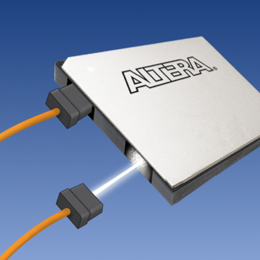
What if we could get that transceiver-to-optics connection right inside the FPGA? Then, the FPGA vendor could handle all the signal integrity issues before the part ever leaves the factory. We’d just plug a nice fiber cable right into our FPGA package, and data would go blasting out to the next chip, the next board, or even to the all-optical backplane that we’ll inevitably want.
That’s exactly what Altera plans to do.
This week, Altera announced plans to build FPGAs with optical transceivers built right into the package. While details of the implementation are not being disclosed yet, we picture a package containing a conventional FPGA with SerDes tranceivers – and those transceivers will be permanently connected to an optical bridge with fiber connections right to the package. This means that board design will suddenly be substantially less complicated, transceiver tuning will become a thing of the past, and Agilent and Tek can lose lots of revenue from all the BERT devices they won’t have to sell us. Overall, this could mean an end to the frustrating process of signal integrity adjustment on every single multi-gigabit connection we make.
Altera says the new technology will dramatically reduce system complexity, cost, and power. On linecard applications, the company foresees replacing pluggable optical modules for short-reach connections (<100m) and increasing port density and bandwidth by orders of magnitude. Today, on a global scale, our fiber connections have considerably more bandwidth than we need. The bottenecks are at the nodes – the switches and transfer points. That’s where the copper still lives, and that’s where Altera’s optical plans come into focus.
Altera says the key to this new technology is the work they’ve already done over the years in transceiver design. Moving the optical module into the package takes one part of the next jump in transceiver development off the table, allowing them to focus on raw speed and power optimization. If the cost of the optical components drops fast enough, that could be a winning bet. With the upcoming 28Gbps transceivers, signal integrity design with copper connections will already be a bear. Beyond that, it could get impractically ugly. Fiber connections direct to the FPGA offer hope of ending that problem for good.
Altera claims they’ll have a demonstration of this new technology in 2011. No specific timetable has been given. As exciting as a demonstration might be, however, the real test of this technology will be the company’s ability to deliver it in volume at a competitive price point. FPGAs with optical connections built in need to be at least as cheap as the components purchased separately.
There are infrastructure and ecosystem challenges brought with this advance, too, obviously. The ability to connect optics directly to FPGAs is just one part of the puzzle. Ultimately, we’ll want cost-effective, high-performance, interesting things on the other end of those optical connections as well. If the copper backplane goes out of fashion, we’ll need a new optical backplane to take its place – and that will certainly bring new challenges of its own. We will also face issues of co-existence and migration from the current copper-based world to the light-and-fast fiber-linked FPGAs of the future.
During the interim, transitional hybrids will probably be ugly, confusing, and exciting – all at the same time. Replacing high-speed copper connections with optics is a discontinuity in design. Discontinuities pose engineering challenges that are far different from the “normal” evolutionary change. While we have become oddly accustomed to the Moore’s Law migration of exponential density, speed, and power improvements, we’re less adept at handling shifts in the underlying fundamentals.
Back when geometries were first dipping below one micron, we had the perception that silicon was about to “run out of gas,” and that we might need to migrate to other materials like gallium arsenide. Even though a niche market emerged for that technology, silicon had much longer legs than we’d anticipated, and it’s still with us today. Now, we’re predicting the demise of copper for high-speed interconnect. While the future for fiber looks bright, it is also possible that our predictions are once again premature. The only way to find out, however, is to try out some of these newfangled optically-connected FPGAs. Bring ‘em on, Altera!


