

It wasn’t very long ago that managing off-chip interconnect was a no-brainer. The interconnect path was very straightforward. It started at a pad on the chip, went out through a bond wire then connected to a metal lead, which connected to the PCB. The number of “interfaces” was small; a total of 4 counting the pad on the chip, the bond wire, the metal lead and the PCB, as illustrated in Figure 1.
Figure 1: Diagram of a classic IC leadframe package
Interfacing Gets More Complex
Flip-chips and routable package substrates introduced additional interfaces into the mix. The C4 bumps, re-distribution layer (RDL) routing, and package routing (including vias) added additional interfaces, driving up the complexity of managing the off-chip interconnect path. Additionally, I/O were getting faster and faster, meaning designers now had to pay more attention to off-chip signal integrity. Designers now had to manage and optimize a much more complex network of off-chip interfaces for routability, signal integrity, and power delivery.
Just as design teams were refining their flows and methodologies for flip-chip development, a new technology started creeping into the mix — through silicon via (TSV) interconnect. TSV is the key technology driving 2.5D and 3D ICs and it further complicates the off-chip interconnect path. Designers now have to manage three additional off-chip interfaces — TSVs, micro bumps, and in the case of 2.5D ICs, silicon interposers. Figure 2 shows a typical 2.5D package.
Figure 2: Increasing complexity of the 2.5D-IC package makes the external interface yet more complex
The off-chip interconnect path in the case of a 2.5D IC can consist of a least eight different interfaces! Starting at the I/O, the signal path then goes through the RDL to the micro bump then onto the silicon interposer. Now it gets interesting; some signals will connect to another IC(s) placed on the interposer and some signals will connect to a TSV that in turn is connected to a C4 bump then out through the package substrate routing into the package pin, and finally onto the PCB.
Managing this complex off-chip interconnect path is one thing. Optimizing this path for routability, signal integrity, and power delivery is where the real challenge lies. This has forced design teams at many semiconductor companies to begin research on alternatives to their current error prone spreadsheet-based methodologies.
A Connectivity Definition Challenge
The first bridge to cross when architecting a new methodology that can support this complex off-chip network is to define how the connectivity (netlist) between interfaces will be captured and managed. There are a few key areas of technology that should be considered. First, the solution must support the ability to automate pin mapping across the different interfaces. This is important because the signal name rarely stays the same as it traverses across the various off-chip interfaces, including the package and PCB. It is important that the electrical path of the signal stay intact even though the name will likely change from interface to interface.
The second thing that is important to consider is the method of capturing connectivity. There are two basic approaches: text based and graphical based. In the majority of cases the preferred method will be text based for defining the connectivity between chips and their off-chip interfaces. However, in some cases one or more of the off-chip interfaces may include more than just basic connectivity. As an example, for an RF application, the interposer might include a filter circuit made up of spiral inductors and interdigital capacitors. For these types of situations the designer may want to capture the circuit using a traditional graphical schematic. Therefore, it is important that the solution used to capture the connectivity for the off-chip interfaces support both modes of capture in a single tool.
Additionally, the solution must support the ability to capture the connectivity for multiple physical designs. Due to the nature of this probable cross-domain methodology, the user would likely want to partition the connectivity across multiple physical design domains including the chip(s), interposer(s), and package substrate for physical implementation. This same solution would also be required to support the different physical and electrical constraints that would be typical in an off-chip interconnect network such as timing, impedance, and termination.
Optimizing the Interconnect Path
The solution discussed above would take care of the “management” side of chip to chip and off-chip connectivity, but what about optimizing the interconnect path between multiple chips in a stack and/or through all of the off-chip interfaces required in a 2.5D configuration? There are several things to consider when optimizing the off-chip interconnect path. For the case of two chips in a 3D stack, the locations and signal assignment of the TSVs and micro bumps is key to reducing — or even eliminating — any redistribution routing (RDL) between the chips. As mentioned above, the bigger challenge may be for 2.5D configurations. Optimization must traverse more off-chip interfaces including a silicon interposer for these designs.
When discussing optimization specific to off-chip interfaces, the first thing to come to mind is typically optimization for routability. This type of optimization can typically lead to on-chip metal layer reduction, interposer metal layer reduction and package substrate layer reduction (See figure 3 and figure 4). Taken all they way out to the PCB, it can also reduce layer count on the final board. All can lead to significant cost reduction. However, careful attention must also be given to signal integrity and power delivery when doing optimization.
For example, overlooking the effects of simultaneous switching outputs (SSO) while optimizing a group of signals for routability might result in a package substrate that has fewer signal layers, but likely would lead to a substrate that required additional power layers. The net cost of the package in this case would likely not change. Therefore, it is important to understand the electrical characteristics along with the physical locations of pins when optimizing the off-chip interconnect path.
To effectively optimize a signal path that traverses multiple off-chip interfaces, you must be able to view all of the interfaces in a single graphical window. Starting with the chip(s), abstract models should be used as a substitute for full chip layouts to improve performance. These models include the physical locations of structures such as I/O pads, TSVs and micro bumps. I/O buffer data is required in the model to support SSO based optimization. Rules for high-speed signals, such as impedance and timing, as well as termination requirements should be included in this model or entered into the centralized constraint database mentioned above.
Finally, a comprehensive set of pin compatibility rules should be included in the model to drive the physical optimization of the off-chip interconnect path. In short, a virtual die model (VDM) would replace the full chip layout for the purpose of off-chip interface optimization. The VDM along with other off-chip interfaces such as bump arrays, interposers, the package substrate, and even board level devices (including breakout routing) would be displayed in a single graphical window, allowing designers from all physical domains an easy way visualize the complete off-chip interconnect path. Flight lines graphically indicate connectivity between the different interfaces.
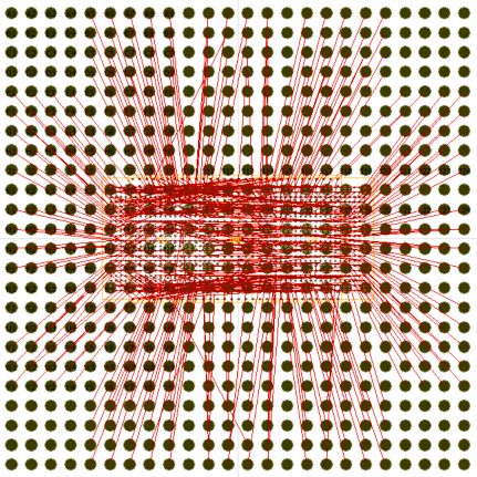
Figure 3: Without optimization, interposer and package interconnect paths can get very messy
and add cost to the chip
Figure 4: With an optimized chip(s), interposer and package interconnect paths are much simpler, often allowing elimination of layers and the need for redistribution routing
This type of solution would allow designers across multiple design domains the ability to choose an interface or a group of signals and easily optimize the complete path. Having the complete off-chip network in a single environment greatly simplifies the signal optimization task by allowing all interfaces to be optimized concurrently. Ideally, automatic optimization algorithms would simultaneously evaluate a signal path(s) for routability, signal integrity, and SSO while reassigning pins throughout the off-chip network. The integrity of the chip’s floorplan would be preserved through the use of the VDM (described above), while allowing the flexibility to create the optimal signal path through the network of off-chip interfaces. Extending this methodology out to the PCB, would allow design teams to create chips and packages that are completely optimized for the boards that they will eventually sit on. It’s easy to see how this approach would greatly reduce the complexity of PCB layout, resulting in a less expensive (reduced layers) board designed in a shorter amount of time.
If properly implemented, this type of methodology would lead to a reduction of interconnect length and improved signal quality through the complete network of off-chip interfaces out through the package pin and onto the PCB. It is easy to see how this approach would lead to metal layer reduction for redistribution across chips and interposers. In addition, tremendous cost savings would likely be seen for the package substrate as well as the PCB.


8 thoughts on “3D ICs”