

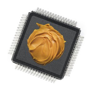
You probably remember the TV commercials. Two strangers randomly collide – co-mingling their confections in a fictitious fortuitous coincidence – giving the world the magic that is Reese’s Peanut Butter Cups. It’s a lie, but fact emerges from farce – chocolate and peanut butter make a very nice combination.
FPGA fabric and optimized circuit blocks make a very nice combination, too. Why settle for lower performance, lower density, and higher power consumption for the parts of your circuit that do not require the flexibility of FPGA fabric? Why pour concrete and lock down chunks of your design in hard-core cells that are likely to change or require multiple variants?
Clearly, the ideal chip combines optimized, hard-core circuit blocks with copious quantities of programmable fabric for flexibility. Hard-core logic exploits the full potential of the latest-generation semiconductor process, minimizing power and area while maximizing performance. Programmable logic fabric allows the design to morph and adapt without the staggering expense of multiple mask sets. Like peanut butter and chocolate, the combination is far more than the sum of the two parts.
As process geometries get smaller and NREs and mask costs grow exponentially larger, this argument becomes even more compelling. If you’re building an application-specific chip, but you need several variants for different situations, you don’t want to take the hit of a different chip design for each one. By having the variable part in FPGA fabric, you can design a single chip instead of many, and save millions (or tens of millions) in the process.
We must, therefore, have FPGA fabric blocks available to embed in our custom ICs.
Ah, not so fast there, Custom SoC Man. You see, this is not a new idea. For at least a decade, designers have been drooling about the prospect of programmable fabric on their ASICs, SoCs, and ASSPs. At first, there were issues like patents and process incompatibility, but those have long since disappeared. It would be a fairly straightforward matter today to pop open the jar of programmable logic fabric and spread some around in all the blank spots on your SoC design. (You’ll almost certainly have some blank spots, because your design is pad-limited, right?)
Why can’t we do that, then?
It turns out the magic is not in the fabric. Fabric is easy. The look-up-table is no longer logic-design wizardry. As much as Xilinx and Altera and the rest still both boast about their fabric being faster, smaller, lower power, or whatever – the real keys to the kingdom of programmable logic are tools, IP, and support. As countless failed FPGA start-ups have proven, having a better idea for FPGA fabric won’t turn you into a successful programmable logic company. The thing that wins designs for an FPGA company is enabling the customer/designer to get the fabric to do what they want as easily as possible, and with minimal risk. Doing that requires the magic trio of tools, IP, and support.
Right now, the FPGA companies are the only ones in the world with the wherewithal to enable engineers to get programmable logic fabric to work. Furthermore, their advantage in that department is staggering. Getting a working, commercially-viable, deployable design flow for FPGA fabric requires years of development and customer experience. No well-funded intruder can come in and capture that capability by pouring engineering resources on the problem either. In “The Mythical Man Month,” Fred Brooks pointed out that “nine women can’t make a baby in one month.” For a new entity to get a customer-ready FPGA flow going, we’d have to modify Brooks’s observation to something like “nine men can’t make a baby… ever.”
It turns out that the solution to our magic mixture of FPGA fabric and hard logic is coming from the other side – the only side it can come from, in fact. It is coming from the FPGA companies. Instead of putting FPGA fabric in our custom SoC designs, we are getting custom SoC in our FPGAs. The programmable logic industry long ago abandoned the “pure” FPGA – a big field of programmable fabric surrounded by IO. They saw the advantage in hardening common functions like multipliers, memory, IO (of course), and even processors. Today’s FPGA is already a hybrid part with optimized standard cells and FPGA fabric living on the same die.
Moving forward, however, it’s clear that the FPGA side is raising their game. Major FPGA companies like Xilinx and Altera have announced the addition of entire embedded processing subsystems on their upcoming devices. Smaller players like QuickLogic, Lattice, and Actel all already sell parts that are not marketed as FPGAs, but that take advantage of the flexibility of FPGA fabric to deliver differentiated value to the customer. These super-flexible ASSP-like devices (QuickLogic wants us to call them CSSPs) hit a sweet spot of optimized hard-core design mixed with FPGA flexibility.
ASSP companies are already hitting an economic wall where the cost and risk associated with developing a new chip on the latest process make all but the highest-volume applications non-starters. Most ASIC design in the world has stopped already – with the market segmenting into two camps of survivors – mega-funded companies with gigantic-volume products that can afford latest-generation custom SoC development, and niche players that continue doing ASIC design with older-generation processes. This leaves an enormous gap that can be filled by hybrid FPGA/hard-core devices and nobody but the FPGA companies with the required technology and infrastructure to sell and support them.
This positions FPGA companies in the best place they’ve ever been – a place from where they could capture huge segments of the standard parts and ASSP business with semi-standard parts that include FPGA fabric for application-specific customization. Short of buying an established FPGA company, this could leave many traditionally-strong semiconductor suppliers out in the cold. FPGA companies won’t get this for free, however. The big guys will have to adopt some of the tactics of smaller players like QuickLogic to win sockets in markets where the FPGA design process is still a bit too scary. Instead of today’s still-very-general-purpose FPGAs, we’ll need to see more devices with a narrower application focus that can boot the incumbent solutions convincingly without too much general-purpose overhead lying around on the die. Of course, with each passing process generation, the cost of that overhead shrinks, and the cost of developing the traditional alternative solutions goes up. It will be interesting to watch.


