

 We’ve talked about photonics before and we’ve talked about nanoimprint lithography (NIL) before. Creating silicon photonics features requires masking, which requires lithography, and so it might not be a surprise to hear that all different kinds of lithography techniques – including NIL – were being explored for photonics.
Which is how I went into a discussion with EV Group at Semicon West. But that’s not what the story is at all. This is not about patterning resists to pattern silicon for silicon photonics – this is about building photonics structures directly out of… various other non-silicon materials, using imprint as a direct patterning approach.
I can’t help but think about NIL as if it were printing vinyl albums. Which are black. (Except a few novelty ones.) Even if printing resist, any resist I remember seeing way back in my fab days was distinctly not transparent. So picturing these materials as conduits for light is something my brain, well, resists.
But it’s apparently true: many of the materials available to be imprinted happen to be transparent (at suitable wavelengths). So you can build the conduits right on the surface of the wafer – no further etching required.
EVG notes that there are a number of high-volume apps for NIL these days:
- Polarizers
- Patterns for extracting more energy out of LEDs
- Biotech (they can’t say specifically what)
- And… one more big one coming that they also couldn’t talk specifically about.
Meanwhile, they’ve also teamed with Leti in a so-called INSPIRE program to further develop techniques and applications for NIL. You can find more about this in their announcement.
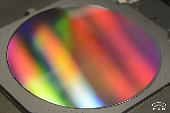
(Image courtesy EV Group)


