While wandering the halls of SPIE Advanced Litho, I had a conversation with Synopsys’s Tom Ferry about their focus for the leading edge of lithography.
He addressed several areas, many of which reflect progress on existing notions. Compact models are getting less… well, compact as compared to so-called “rigorous” models. Given the number of effects to be covered, Synopsys is moving to rigorous models to improve predictability.
They’re also making progress on DSA support as well as reducing mask write times. The topic that’s a bit different, however, is inverse lithography technology (ILT). While not new, it’s always been too compute-intensive (read “expensive”) for commercial use. That’s changing both as its value grows at aggressive nodes and as computing capabilities improve.
Some background: for years, now, we’ve been adorning our masks with little features (called “assist features”, or AF) that will never print. Which is good, because we don’t want them on the actual mask. What they do is monkey with the light coming through other features of the mask to make the printed versions of those other features sharper or less distorted by the craziness that light undergoes with these tiny dimensions.
This is the domain of optical proximity correction, or OPC. Algorithms have typically been empirical: sophisticated heuristics based on what we know works and doesn’t work are built into algorithms that scour a mask for opportunities to improve fidelity.
But there’s been an, until now, academic notion floating around for a while. The process of exposing a wafer converts the mask pattern to a wafer pattern. You can think of this as a mathematical function – I’ll call it E (for Exposure). If the mask pattern is M and the resulting wafer pattern is W, then W=E(M).
The idea is to start with the ideal W and work backwards find the corresponding ideal M – which amounts to finding the inverse function of E (call it E-1). So then M= E-1(W). It’s kind of like pre-equalization.
There are a couple practical problems, however. There are some parts of the E function (which includes exposure dose, focus, photoresist, development, washing, etc., etc.) that may be well understood from a practical standpoint, but not to the point of being able to derive a mathematical function for them.
But here’s the other thing: according to a paper from Luminescent Technologies in 2006, (a company since acquired by – I’ll bet you already guessed it – Synopsys in 2012), there is no one unique inverse of E. From a practical standpoint, that’s saying that there are different ways to decorate a mask with these unprintable features and essentially get the same result. And some solutions may be easier or harder to manufacture.
So that sort of nukes the idea of a single E-1. Instead, you can look at the difference between a given wafer pattern W and the ideal desired wafer pattern – let’s call it W+. They turn this into an optimization problem where they minimize (W+-W) while also taking into account various other costs – like ease of manufacturing.
Critically, this is a “pixel-based” solver approach rather than an edge- or feature-based approach. This apparently widens the possible solution space, allowing for results that might not be at all obvious or intuitive – even to an experienced litho dude.
In addition, it turns out the problem can be fractured so that distributed computing can make the solution tenable. That’s not to say, however, that it’s easy – it’s still a bear to do. So they’re targeting only the most challenging geometries with this, integrating it into a general OPC flow, where the old methods are still used where possible.
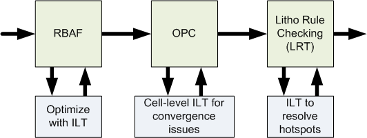
Synopsys’s approach is to
- Use ILT before OPC for optimizing rule-based assist features (RBAF)
- Use ILT at the cell level where OPC has convergence problems
- Use ILT to address any hotspots after OPC.

You’ll see this at the 10-nm and below nodes; Synopsys has this close to being ready for prime time. (I know, you might think that 10 nm is a long way from prime time, but the folks developing these nodes need to be able to create masks…)


