We used to be ok with the verification silos we grew up with. You’ve got your simulation guys over here helping with circuit and block verification. You’ve got your emulation group over there checking out larger system chunks or running software. In yet another corner, you’ve got your virtual platforms running software.
But really, there can be a lot of rework involved as an SoC migrates from being individual bits and pieces, individually tested, to a unified system, holistically tested. So a group at Accellera has formed to standardize a stimulus format so that verification intent and stimulus can be ported to different environments.
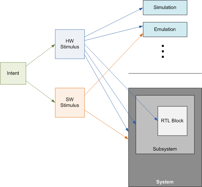
The scope here appears to be twofold. On the one hand, you’ve got different verification methodologies: simulation, emulation, etc. The different platforms may expect different inputs – even if just variations. On the other hand, this also appears to be about scale – blocks and components vs. complete systems.
One of the big differentiators at the system level is the use of software to test out the hardware platform. Note that this is different from using a virtual platform to test software: in that case, it’s the software that’s being tested with a “known good” platform model. The focus of this stimulus effort is more about verifying the platform itself; when software is used for that, then it’s the software that’s “known good.” So, of the silos I mentioned above, that last one seems unlikely to be affected. Then again, it’s different from the others, since it’s not about hardware verification.
Because the low-level stimulus details for, say, simulation will be different from that for software, this is more about capturing intent and verification scenarios for automated generation of the actual stimulus that makes its way into the test environment.
The first meeting just happened a week ago; if it’s an activity you’d like to be involved in, now’s a good time to jump in. Apparently a roadmap hasn’t yet been sketched out, so it’s still early days.
You can find more in their announcement.