Heat has got to be one of the most annoying side-effects of doing useful electrical work. The more work we do, the more things heat up, changing the characteristics of the circuitry and, if we’re not careful, leading to early end-of-life or outright failure.
It’s heat that’s part of why we’ve gone to multicore instead of simply ratcheting up microprocessor clock frequencies forever. Greater dissipation is one reason we end up with power transistors that are larger than they need to be for electrical reasons. And when 3D ICs were first trotted out as an idea some years back, one of the immediate questions was how heat would be removed from the center of the stack.
We do lots of things to mitigate heat: elaborate cooling systems, heat spreaders in packages, and modified silicon designs to reduce thermal density. All of which add cost in one way or another.
Well, for one application, a different solution has been proposed. Gallium nitride (GaN) is a wide-bandgap material used for high-electron-mobility transistors (HEMTs) in high-power RF applications – radar, cellular base station radios, satellite radios, and the like. The GaN typically sits over a silicon substrate, with a transition layer to ease stresses due to mismatches in the crystal lattice spacing of the two materials.
These circuits have localized hot spots that have to be carefully managed (with heat flux that Element Six says rivals that of the sun). Metal is typically used to wick away heat, and we all know that copper is a good conductor of heat, topping out at about 400 W/mK. But we have looked at one material that is a far better heat conductor than copper: diamond. Diamond can conduct heat in the range of 1000-2000 W/mK.
Unlike copper, which uses electrons to conduct the heat away, diamond does so through vibrations of the crystal lattice – so-called phonons (a fictitious particle for analysis of crystal vibrations and their properties and propagation). So higher-quality crystals will spread heat better than high-defect crystals or polycrystalline depositions.
Element Six does sell diamond heat spreaders that can be included under standard GaN/silicon or GaN/SiC (silicon carbide) circuits, and they’ll help, but they place the diamond material some hundreds of microns away from the transistor gate, where the heat originates.
A better solution, they say, is to have a transistor consisting of GaN on a diamond substrate rather than a silicon substrate. The standard transition layer between silicon and GaN is also a barrier to a conductive path from gate to substrate, so they’ve eliminated that as well, replacing it with their own “secret sauce” of a transition layer.
By doing this, you’ve now got the transistor gate about 1 micron away, roughly tripling the heat dissipation.
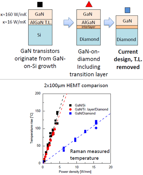
Upper image courtesy Element Six; graph credit Professor Martin Kuball, Bristol University
Their actual production process leverages GaN/Si layers already in production. They put a handle wafer on top, flip them over, remove the silicon substrate and the transition layer, and then add their own transition layer and grow a polycrystalline diamond substrate. That substrate is strong, but it’s not thick enough for fab handling, so they temporarily affix another diamond wafer, which is eventually removed and re-used up to 10 times. (They’re working on a cheaper handle wafer solution for this last bit.)
GaN on Diamond allowed Triquint and Raytheon to achieve a three-fold improvement in power density as compared to GaN/SiC, allowing them to meet a challenge set by DARPA.
You can read more about the Raytheon achievement in their announcement.