

A while back Micralyne announced a MEMS reference process. There are a few of these running around: attempts to achieve – or at least grasp at – a standard process that can address a wide range of MEMS devices.
Most of Micralyne’s processes are confidential, per their customer relationships, in typical MEMS style. What they did here was to take a “neutral” improved version of what they do well and open it up. They’re not sure that customers will simply line up and use that process in high-volume production outright, but at the very least it’s a conversation starter and a way for them to show their capabilities without divulging secrets.
Micralyne’s strength is primarily optical MEMS: mirrors and comb drives and such. Those feature large in their process, but, in order to be a bit more general, they added some inertial devices, like a 2-axis (but not a 3-axis) accelerometer and a gyro, as well as some biomedical devices.
It’s a two-wafer process (plus handles); cavities are etched into the base wafer and the top wafer; the top wafer is inverted and fusion-bonded to the bottom wafer, after which the top-wafer handle is removed. From the top, release is performed and then metal is laid down. This metal step pertains in particularly to giving mirrors a nice reflective surface.
As a complete aside, in the discussion of their optical capabilities, there was repeated mention of “hitless” functionality with respect to the mirrors. I actually had a hard time finding out what this meant, and a conversation with Micralyne helped clarify. For any of you who are, like me, not steeped in optical, this is a way of changing optical routing in an optical switch without interfering with other channels.
It’s actually a pretty simple concept. Below I show a scenario with various fibers being routed to various other fibers via the gold mirrors. In particular, fiber 3 routes to fiber 1 (moving bottom to top). Let’s say we want to reroute that so that fiber 3 now routes to fiber 6. If we just move the mirror across, then the light stream from fiber three will interfere with all of the other receiving channels as it scans across (which I’ve tried to illustrate on the right, with the stars indicating interference as the beam moves; at the particular moment shown, it’s made it as far as target fiber 4 on its way to 6).
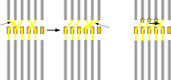
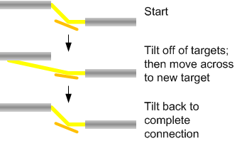
So the hitless idea is that you simple tilt the mirror in the orthogonal direction first so that it’s no longer targeting the receiving fibers. You can then sweep it across to the new target; the light is now moving under the other beams and doesn’t interfere. Once over in the new position, you then bring the beam back up to its normal working position and the connection is made (with no disturbance to the others).
You can find more info in their release and whitepapers.


