editor's blog
Subscribe Now

A Buttable X-Ray Detector

Most image sensors receive light that has passed through a lens of some sort. This means that a large area can be photographed, for example, and sensed on a chip that is extremely small by comparison with the scene itself.

Not so with medical X-ray imaging. The target sensor gets a full-sized image. Not so hard for dental work, but more challenging for mammography or other full- or partial-body scans.

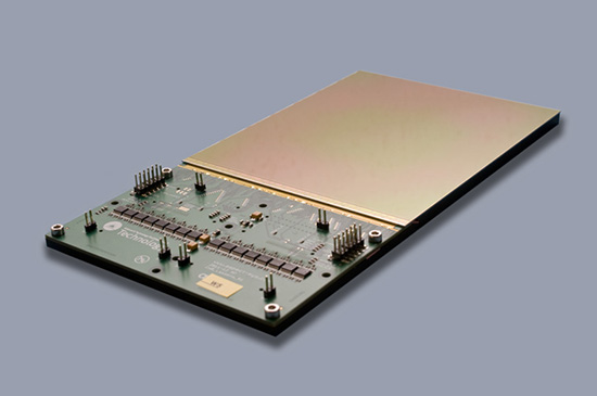
It’s typically hard, therefore, to provide a solid-state target that can provide seamless coverage. No matter how large they’ve been, they’ve had pixel addressing circuitry on two sides, meaning that you can’t tile them together. (At least not without having “blind stripes” where the decode logic blocks meet up…)

TowerJazz and Tanner worked together with the UK Science and Technology Facility Council’s Rutherford Appleton Labs to develop a unique decoding scheme that allowed them to restrict themselves to only one edge for the circuitry, allowing pixels all the way up to the other three edges. That means that you can tile them in any 2xN configuration.

With each sensor being basically the size of a 200-mm wafer (6.7 Mpixels), they can handle mammography applications with a 2×2 arrangement; longer targets are possible for other applications.

As to how they did the decoding? Yeah… they’re being coy about that. It seems to be largely an analog approach, which is where Tanner contributed to the process. But more details weren’t forthcoming…

You can read more in their release.

EDAS0088-STFCimagesensor_550px.jpg

Leave a Reply

featured blogs
Apr 19, 2024
Data type conversion is a crucial aspect of programming that helps you handle data across different data types seamlessly. The SKILL language supports several data types, including integer and floating-point numbers, character strings, arrays, and a highly flexible linked lis...
Apr 18, 2024
Are you ready for a revolution in robotic technology (as opposed to a robotic revolution, of course)?...
Apr 18, 2024
See how Cisco accelerates library characterization and chip design with our cloud EDA tools, scaling access to SoC validation solutions and compute services.The post Cisco Accelerates Project Schedule by 66% Using Synopsys Cloud appeared first on Chip Design....

featured video

How MediaTek Optimizes SI Design with Cadence Optimality Explorer and Clarity 3D Solver

Sponsored by Cadence Design Systems

In the era of 5G/6G communication, signal integrity (SI) design considerations are important in high-speed interface design. MediaTek’s design process usually relies on human intuition, but with Cadence’s Optimality Intelligent System Explorer and Clarity 3D Solver, they’ve increased design productivity by 75X. The Optimality Explorer’s AI technology not only improves productivity, but also provides helpful insights and answers.

Learn how MediaTek uses Cadence tools in SI design

featured chalk talk

Littelfuse Protection IC (eFuse)
If you are working on an industrial, consumer, or telecom design, protection ICs can offer a variety of valuable benefits including reverse current protection, over temperature protection, short circuit protection, and a whole lot more. In this episode of Chalk Talk, Amelia Dalton and Pete Pytlik from Littelfuse explore the key features of protection ICs, how protection ICs compare to conventional discrete component solutions, and how you can take advantage of Littelfuse protection ICs in your next design.
May 8, 2023
41,000 views